- 您现在的位置:买卖IC网 > PDF目录10516 > AD677KNZ (Analog Devices Inc)IC ADC 16BIT SAMPLING 16DIP PDF资料下载
参数资料
| 型号: | AD677KNZ |
| 厂商: | Analog Devices Inc |
| 文件页数: | 5/16页 |
| 文件大小: | 0K |
| 描述: | IC ADC 16BIT SAMPLING 16DIP |
| 标准包装: | 1 |
| 位数: | 16 |
| 采样率(每秒): | 100k |
| 数据接口: | DSP,串行 |
| 转换器数目: | 1 |
| 功率耗散(最大): | 480mW |
| 电压电源: | 模拟和数字,双 ± |
| 工作温度: | 0°C ~ 70°C |
| 安装类型: | 通孔 |
| 封装/外壳: | 16-DIP(0.300",7.62mm) |
| 供应商设备封装: | 16-PDIP |
| 包装: | 管件 |
| 输入数目和类型: | 1 个单端,双极 |
| 配用: | AD677-EB-ND - BOARD EVAL SAMPLING ADC AD677 |
AD677
REV. A
–13–
The standard deviation of this distribution is approximately
0.5 LSBs. If less uncertainty is desired, averaging multiple con-
versions will narrow this distribution by the inverse of the square
root of the number of samples; i.e., the average of 4 conversions
would have a standard deviation of 0.25 LSBs.
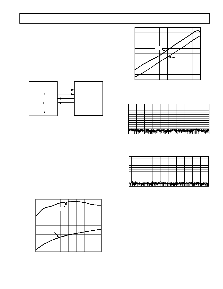
DSP INTERFACE
Figure 10 illustrates the use of the Analog Devices ADSP-2101
digital signal processor with the AD677. The ADSP-2101 FO
(flag out) pin of Serial Port 1 (SPORT 1) is connected to the
SAMPLE line and is used to control acquisition of data. The
ADSP-2101 timer is used to provide precise timing of the FO
pin.
ADSP-2101
FO
AD677
SAMPLE
SERIAL
PORT 0
CLK
BUSY
SCLK0
DR0
RFS0
DT0
TFS0
SDATA
Figure 10. ADSP-2101 Interface
The SCLK pin of the ADSP-2101 SPORT0 provides the CLK
input for the AD677. The clock should be programmed to be
approximately 2 MHz to comply with AD677 specifications. To
minimize digital feedthrough, the clock should be disabled (by
setting Bit 14 in SPORT0 control register to 0) during data ac-
quisition. Since the clock floats when disabled, a pulldown resis-
tor of 12 k
–15 k should be connected to SCLK to ensure it
will be LOW at the falling edge of SAMPLE. To maximize the
conversion rate, the serial clock should be enabled immediately
after SAMPLE is brought LOW (hold mode).
The AD677 BUSY signal is connected to RF0 to notify
SPORT0 when a new data word is coming. SPORT0 should be
configured in normal, external, noninverting framing mode and
can be programmed to generate an interrupt after the last data
bit is received. To maximize the conversion rate, SAMPLE
should be brought HIGH immediately after the last data bit is
received.
102
9.5
86
82
2.5
90
94
98
8.5
4.5
3.5
V
REF – Volts
dB
106
5.5
6.5
7.5
THD
S/(N+D)
10.0
Figure 11. S/(N+D) and THD vs. VREF, fS = 100 kHz (Calibra-
tion is not guaranteed below +5 VREF)
INPUT LEVEL – dB
105
10
0
40
20
–70
30
–80
70
50
60
80
90
100
–10
–20
–30
–40
–50
–60
THD
S/(N+D)
dB
Figure 12. S/(N+D) and THD vs. Input Amplitude,
fS = 100 kHz
0
–20
–40
–60
–80
–100
–120
–140
0
51015
20
25
30
35
40
45
50
FREQUENCY – kHz
AMPLITUDE
–
dB
Figure 13. 4096 Point FFT at 100 kSPS, fIN = 1 kHz,
VREF = 5 V
0
–20
–40
–60
–80
–100
–120
–140
0
5
10
15
20
25
30
35
40
45
48
FREQUENCY – kHz
AMPLITUDE
–
dB
Figure 14. 4096 Point FFT at 100 kSPS, fIN = 1 kHz,
VREF = 10 V
相关PDF资料 |
PDF描述 |
|---|---|
| VI-J22-MY-F2 | CONVERTER MOD DC/DC 15V 50W |
| UP050B821K-B-B | CAP CER 820PF 50V 10% AXIAL |
| VI-JWB-MY-F2 | CONVERTER MOD DC/DC 95V 50W |
| MAX3033ECUE+ | IC RS-422 TRANSMIT QUAD 16TSSOP |
| MS3110P12-10P | CONN RCPT 10POS WALL MNT W/PINS |
相关代理商/技术参数 |
参数描述 |
|---|---|
| AD677KR | 功能描述:IC ADC 16BIT 100KSPS 28-SOIC RoHS:否 类别:集成电路 (IC) >> 数据采集 - 模数转换器 系列:- 标准包装:1 系列:- 位数:14 采样率(每秒):83k 数据接口:串行,并联 转换器数目:1 功率耗散(最大):95mW 电压电源:双 ± 工作温度:0°C ~ 70°C 安装类型:通孔 封装/外壳:28-DIP(0.600",15.24mm) 供应商设备封装:28-PDIP 包装:管件 输入数目和类型:1 个单端,双极 |
| AD677KR-REEL | 功能描述:IC ADC 16BIT SAMPLING 28-SOIC RoHS:否 类别:集成电路 (IC) >> 数据采集 - 模数转换器 系列:- 标准包装:1 系列:- 位数:14 采样率(每秒):83k 数据接口:串行,并联 转换器数目:1 功率耗散(最大):95mW 电压电源:双 ± 工作温度:0°C ~ 70°C 安装类型:通孔 封装/外壳:28-DIP(0.600",15.24mm) 供应商设备封装:28-PDIP 包装:管件 输入数目和类型:1 个单端,双极 |
| AD677KRZ | 功能描述:IC ADC 16BIT 100KSPS 28-SOIC RoHS:是 类别:集成电路 (IC) >> 数据采集 - 模数转换器 系列:- 标准包装:1 系列:- 位数:14 采样率(每秒):83k 数据接口:串行,并联 转换器数目:1 功率耗散(最大):95mW 电压电源:双 ± 工作温度:0°C ~ 70°C 安装类型:通孔 封装/外壳:28-DIP(0.600",15.24mm) 供应商设备封装:28-PDIP 包装:管件 输入数目和类型:1 个单端,双极 |
| AD677KRZ-REEL | 功能描述:IC ADC 16BIT 100KSPS 28-SOIC RoHS:是 类别:集成电路 (IC) >> 数据采集 - 模数转换器 系列:- 标准包装:1 系列:- 位数:14 采样率(每秒):83k 数据接口:串行,并联 转换器数目:1 功率耗散(最大):95mW 电压电源:双 ± 工作温度:0°C ~ 70°C 安装类型:通孔 封装/外壳:28-DIP(0.600",15.24mm) 供应商设备封装:28-PDIP 包装:管件 输入数目和类型:1 个单端,双极 |
| AD677TD | 制造商:未知厂家 制造商全称:未知厂家 功能描述:MICROCIRCUIT, DIGITAL-LINEAR, FAST, SERIAL, 16-BIT, A/D CONVERTER, MULTICHIP SILICON |
发布紧急采购,3分钟左右您将得到回复。