- 您现在的位置:买卖IC网 > PDF目录11657 > AD694BRZ-REEL (Analog Devices Inc)IC TRANSMITTER 4-20MA 16-SOIC PDF资料下载
参数资料
| 型号: | AD694BRZ-REEL |
| 厂商: | Analog Devices Inc |
| 文件页数: | 10/16页 |
| 文件大小: | 0K |
| 描述: | IC TRANSMITTER 4-20MA 16-SOIC |
| 标准包装: | 1,000 |
| 类型: | 电流发送器 |
| 输入类型: | 电压 |
| 输出类型: | 电压 |
| 电流 - 电源: | 23mA |
| 安装类型: | 表面贴装 |
| 封装/外壳: | 16-SOIC(0.295",7.50mm 宽) |
| 供应商设备封装: | 16-SOIC W |
| 包装: | 带卷 (TR) |
Model
AD694JN/AQ/AR
AD694BQ/BR
Min
Typ
Max
Min
Typ
Max
Unit
BUFFER AMPLIFIER
6
Input Offset Voltage
Initial Offset
±150
500
±50
500
V
TMIN to TMAX
±2
±3
±2
±3
V/°C
vs. Supply
80
90
80
90
dB
vs. Common Mode
80
90
80
90
dB
Trim Range
2.5
±4.0
2.5
±4.0
mV
Frequency Response
Unity Gain, Small Signal
300
kHz
Input Voltage Noise (0.1 Hz to 10 Hz)
2
V p-p
Open-Loop Gain
VO = +10 V, RL
≥ 10 k
50
V/mV
Output Voltage @ Pin 1, FB
1
Minimum Output Voltage
1.0
10
1.0
10
mV
Maximum Output Voltage
VS –2.5 V
VS–2 V
VS –2.5 V
VS –2 V
V
NOTES
1The single supply op amps of the AD694, lacking pull down current, may not reach 0.000 V at their outputs. For this reason, span, offset, and nonlinearity are
specified with the input amplifiers operating in their linear range. The input voltage used for the tests is 5 mV to 2 V and 5 mV to 10 V for the two precalibrated
input ranges. Span and zero accuracy are tested with the buffer amplifier configured as a follower.
2Offset at 4 mA out and 0 mA out are extrapolated to 0.000 V input from measurements made at 5 mV and at full scale. See Note 1.
3Nonlinearity is specified as the maximum deviation of the output, as a % of span, from a straight line drawn through the endpoints of the transfer function.
4Voltage reference drift guaranteed by the Box Method. The voltage reference output over temperature will fall inside of a box whose length is determined by the
temperature range and whose height is determined by the maximum temperature coefficient multiplied by the temperature span in degrees C.
5Devices tested at these temperatures with a pass transistor. Allowable temperature range of operation is dependent upon internal power dissipation. Absolute
maximum junction and case temperature should not be exceeded. See section: “Power Dissipation Considerations.”
6Buffer amplifier specs for reference. Buffer amplifier offset and drift already included in Span and Zero accuracy specs above.
Specifications subject to change without notice.
Specifications shown in boldface are tested on all production units at final electrical test. Results from those tests are used to calculate outgoing quality levels.
All min and max specifications are guaranteed, although only those shown in boldface are tested on all production units.
AD694
–3–
REV. B
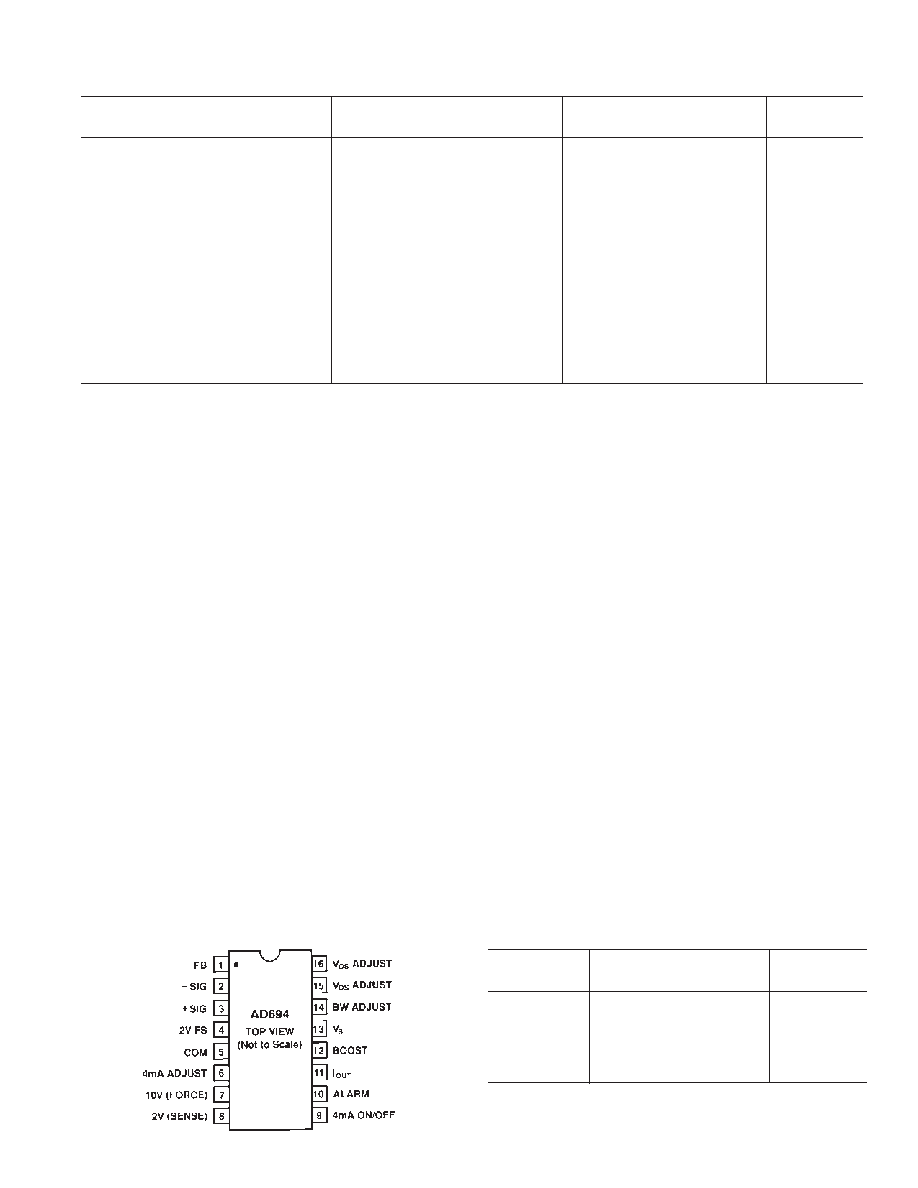
PIN CONFIGURATION (N, R, Q PACKAGE)
ABSOLUTE MAXIMUM RATINGS
Supply Voltage . . . . . . . . . . . . . . . . . . . . . . . . . . . . . . . . . . 36 V
VS to IOUT . . . . . . . . . . . . . . . . . . . . . . . . . . . . . . . . . . . . .36 V
Input Voltage, (Either Input Pin 2 or 3) . . . . . –0.3 V to +36 V
Reference Short Circuit to Common . . . . . . . . . . . . Indefinite
Alarm Voltage, Pin 10 . . . . . . . . . . . . . . . . . . . . . . . . . . . . 36 V
4 mA Adj, Pin 6 . . . . . . . . . . . . . . . . . . . . . . . . . . . . . . . . . . 1 V
4 mA On/Off, Pin 9 . . . . . . . . . . . . . . . . . . . . . . . . 0 V to 36 V
Storage Temperature Range
AD694Q . . . . . . . . . . . . . . . . . . . . . . . . . . –65
°C to +150°C
AD694N, R . . . . . . . . . . . . . . . . . . . . . . . . –65
°C to +125°C
Lead Temperature, 10 sec Soldering . . . . . . . . . . . . . . . 300
°C
Maximum Junction Temperature . . . . . . . . . . . . . . . . . 150
°C
Maximum Case Temperature
Plastic Package (N, R) . . . . . . . . . . . . . . . . . . . . . . . . 125
°C
Cerdip Package (Q) . . . . . . . . . . . . . . . . . . . . . . . . . . 125
°C
ORDERING GUIDE
Temperature
Package
Model
Range
Option
*
AD694JN
0
°C to 70°C
N-16
AD694AQ
–40
°C to +85°CQ-16
AD694AR
–40
°C to +85°C
R-16
AD694BQ
–40
°C to +85°CQ-16
AD694BR
–40
°C to +85°C
R-16
*N = Plastic DIP; Q = CERDIP, R = SOIC
Transistor Count: . . . . . . . . . . . . . . . . . . . . . 75 Active Devices
Substrate Connection: . . . . . . . . . . . . . . . . . . . . to Com, Pin 5
Thermal Characteristics:
Plastic (N) Package:
θ
JC = 50
°C/Watt
θCA (Still Air) = 85°C/Watt
Cerdip (Q) Package:
θJC = 30°C/Watt
θ
CA (Still Air) = 70
°C/Watt
Plastic (R) Package:
θJC = 27°C/Watt
θCA (Still Air) = 73°C/Watt
ESD Susceptibility
All pins are rated for a minimum of 4000 V protection, except
for Pins 2, 3 and 9 which are rated to survive a minimum of
1500 V. ESD testing conforms to Human Body Model. Always
practice ESD prevention.
No pin, other than IOUT (11) and
±Sig (2), (3) as noted, may be permitted to become more negative than Com (5). No pin may be
permitted to become more positive than VS (13).
相关PDF资料 |
PDF描述 |
|---|---|
| VE-JNH-IY-F1 | CONVERTER MOD DC/DC 52V 50W |
| VI-JTK-IW-F2 | CONVERTER MOD DC/DC 40V 100W |
| VE-JNP-IY-F2 | CONVERTER MOD DC/DC 13.8V 50W |
| VI-JTJ-IW-F1 | CONVERTER MOD DC/DC 36V 100W |
| VI-JTH-IW-F3 | CONVERTER MOD DC/DC 52V 100W |
相关代理商/技术参数 |
参数描述 |
|---|---|
| AD694BRZ-REEL7 | 功能描述:IC TRANSMITTER 4-20MA 16-SOIC RoHS:是 类别:集成电路 (IC) >> 接口 - 传感器和探测器接口 系列:- 其它有关文件:Automotive Product Guide 产品培训模块:Lead (SnPb) Finish for COTS Obsolescence Mitigation Program 标准包装:74 系列:- 类型:触控式传感器 输入类型:数字 输出类型:数字 接口:JTAG,串行 电流 - 电源:100µA 安装类型:表面贴装 封装/外壳:20-TSSOP(0.173",4.40mm 宽) 供应商设备封装:20-TSSOP 包装:管件 |
| AD694JN | 制造商:Analog Devices 功能描述:SP Amp INSTR Amp Single 36V 16-Pin PDIP Tube 制造商:Analog Devices 功能描述:TRANSMITTER 420MA SMD DIP16 694 |
| AD694JN | 制造商:Analog Devices 功能描述:SEMICONDUCTORSLINEAR |
| AD694JNZ | 功能描述:IC TRANSMITTER 4-20MA 16-DIP RoHS:是 类别:集成电路 (IC) >> 接口 - 传感器和探测器接口 系列:- 其它有关文件:Automotive Product Guide 产品培训模块:Lead (SnPb) Finish for COTS Obsolescence Mitigation Program 标准包装:74 系列:- 类型:触控式传感器 输入类型:数字 输出类型:数字 接口:JTAG,串行 电流 - 电源:100µA 安装类型:表面贴装 封装/外壳:20-TSSOP(0.173",4.40mm 宽) 供应商设备封装:20-TSSOP 包装:管件 |
| AD694JR | 功能描述:IC TRANSMITTER 4-20MA 制造商:analog devices inc. 系列:- 包装:散装 零件状态:上次购买时间 类型:电流发送器 输入类型:电压 输出类型:电压 接口:- 电流 - 电源:23mA 工作温度:0°C ~ 70°C 安装类型:表面贴装 封装/外壳:16-SOIC(0.154",3.90mm 宽) 供应商器件封装:16-SOIC 标准包装:1 |
发布紧急采购,3分钟左右您将得到回复。