- 您现在的位置:买卖IC网 > PDF目录11657 > AD694BRZ-REEL (Analog Devices Inc)IC TRANSMITTER 4-20MA 16-SOIC PDF资料下载
参数资料
| 型号: | AD694BRZ-REEL |
| 厂商: | Analog Devices Inc |
| 文件页数: | 11/16页 |
| 文件大小: | 0K |
| 描述: | IC TRANSMITTER 4-20MA 16-SOIC |
| 标准包装: | 1,000 |
| 类型: | 电流发送器 |
| 输入类型: | 电压 |
| 输出类型: | 电压 |
| 电流 - 电源: | 23mA |
| 安装类型: | 表面贴装 |
| 封装/外壳: | 16-SOIC(0.295",7.50mm 宽) |
| 供应商设备封装: | 16-SOIC W |
| 包装: | 带卷 (TR) |
AD694
–4–
REV. B
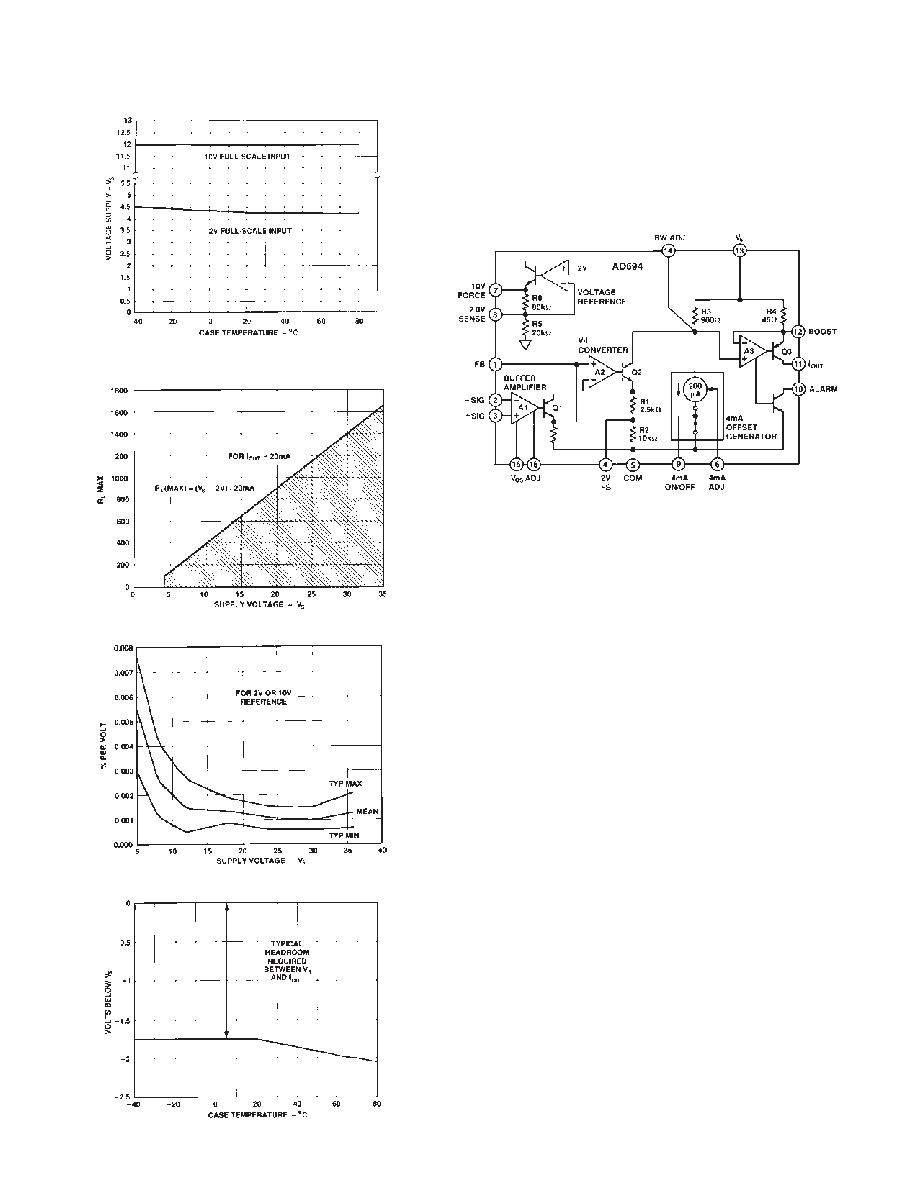
Typical Minimum Supply Voltage vs. Temperature for 2 V
and 10 V Full Scale
Maximum RL vs. Supply Voltage
Voltage Reference Power Supply Rejection
IOUT: Voltage Compliance vs. Temperature
FUNCTIONAL DESCRIPTION
The operation of the AD694 can best be understood by dividing
the circuit into three functional parts (see Figure 1). First, a
single supply input amplifier buffers the high level, single-ended
input signal. The buffer amplifier drives the second section, a
voltage to current (V/I) converter, that makes a 0 to 16 mA sig-
nal dependent current.
Figure 1. Functional Block Diagram
The third section, a voltage reference and offset generator, is re-
sponsible for providing the 4 mA offset current signal.
BUFFER AMPLIFIER
The buffer amplifier is a single supply amplifier that may be
used as a unity gain buffer, an output amplifier for a current
output DAC, or as a gain block to amplify low level signals. The
amplifier’s PNP input stage has a common-mode range that ex-
tends from a few hundred mV below ground to within 2.5 V of
VS. The Class A output of the amplifier appears at Pin 1 (FB).
The output range extends from about 1 mV above common to
within 2.5 V of VS when the amplifier is operated as a follower.
The amplifier can source a maximum load of 5 k
, but can sink
only as much as its internal 10 k
pulldown resistor allows.
V/I CONVERTER
The ground referenced, input signal from the buffer amplifier is
converted to a 0 to 0.8 mA current by A2 and level shifted to
the positive supply. A current mirror then multiplies this signal
by a factor of 20 to make the signal current of 0 to 16 mA. This
technique allows the output stage to drive a load to within 2 V
of the positive supply (VS). Amplifier A2 forces the voltage at
Pin 1 across resistors R1 and R2 by driving the Darlington tran-
sistor, Q2. The high gain Darlington transmits the resistor cur-
rent to its collector and to R3 (900
). A3 forces the level
shifted signal across the 45
resistor to get a current gain of 20.
The transfer function of the V/I stage is therefore:
IV
R1
R2
OUT
PIN1
=×
+
()
20
/
resulting in a 0-16 mA output swing for a 0–10 V input. Tying
Pin 4 (2 V FS) to ground shorts out R2 and results in a 2 V
full-scale input for a 16 mA output span.
The output stage of the V/I converter is of a unique design that
allows the IOUT pin to drive a load below the common (sub-
strate) potential of the device. The output transistor can always
drive a load to a point 36 V below the positive supply (VS). An
相关PDF资料 |
PDF描述 |
|---|---|
| VE-JNH-IY-F1 | CONVERTER MOD DC/DC 52V 50W |
| VI-JTK-IW-F2 | CONVERTER MOD DC/DC 40V 100W |
| VE-JNP-IY-F2 | CONVERTER MOD DC/DC 13.8V 50W |
| VI-JTJ-IW-F1 | CONVERTER MOD DC/DC 36V 100W |
| VI-JTH-IW-F3 | CONVERTER MOD DC/DC 52V 100W |
相关代理商/技术参数 |
参数描述 |
|---|---|
| AD694BRZ-REEL7 | 功能描述:IC TRANSMITTER 4-20MA 16-SOIC RoHS:是 类别:集成电路 (IC) >> 接口 - 传感器和探测器接口 系列:- 其它有关文件:Automotive Product Guide 产品培训模块:Lead (SnPb) Finish for COTS Obsolescence Mitigation Program 标准包装:74 系列:- 类型:触控式传感器 输入类型:数字 输出类型:数字 接口:JTAG,串行 电流 - 电源:100µA 安装类型:表面贴装 封装/外壳:20-TSSOP(0.173",4.40mm 宽) 供应商设备封装:20-TSSOP 包装:管件 |
| AD694JN | 制造商:Analog Devices 功能描述:SP Amp INSTR Amp Single 36V 16-Pin PDIP Tube 制造商:Analog Devices 功能描述:TRANSMITTER 420MA SMD DIP16 694 |
| AD694JN | 制造商:Analog Devices 功能描述:SEMICONDUCTORSLINEAR |
| AD694JNZ | 功能描述:IC TRANSMITTER 4-20MA 16-DIP RoHS:是 类别:集成电路 (IC) >> 接口 - 传感器和探测器接口 系列:- 其它有关文件:Automotive Product Guide 产品培训模块:Lead (SnPb) Finish for COTS Obsolescence Mitigation Program 标准包装:74 系列:- 类型:触控式传感器 输入类型:数字 输出类型:数字 接口:JTAG,串行 电流 - 电源:100µA 安装类型:表面贴装 封装/外壳:20-TSSOP(0.173",4.40mm 宽) 供应商设备封装:20-TSSOP 包装:管件 |
| AD694JR | 功能描述:IC TRANSMITTER 4-20MA 制造商:analog devices inc. 系列:- 包装:散装 零件状态:上次购买时间 类型:电流发送器 输入类型:电压 输出类型:电压 接口:- 电流 - 电源:23mA 工作温度:0°C ~ 70°C 安装类型:表面贴装 封装/外壳:16-SOIC(0.154",3.90mm 宽) 供应商器件封装:16-SOIC 标准包装:1 |
发布紧急采购,3分钟左右您将得到回复。