- 您现在的位置:买卖IC网 > PDF目录11674 > AD698SQ (Analog Devices Inc)IC LVDT SGNL COND UNVRSL 24CDIP PDF资料下载
参数资料
| 型号: | AD698SQ |
| 厂商: | Analog Devices Inc |
| 文件页数: | 11/12页 |
| 文件大小: | 0K |
| 描述: | IC LVDT SGNL COND UNVRSL 24CDIP |
| 标准包装: | 1 |
| 类型: | 信号调节器 |
| 输入类型: | 电压 |
| 输出类型: | 电压 |
| 接口: | LVDT |
| 电流 - 电源: | 15mA |
| 安装类型: | 通孔 |
| 封装/外壳: | 24-CDIP(0.600",15.24mm) |
| 供应商设备封装: | 24-CDIP |
| 包装: | 管件 |
REV. B
–8–
AD698
Note that VOS should be chosen so that R3 cannot have negative
value .
Figure 12 shows the desired response.
+5
+0.1d (INCHES)
–0.1
V
OUT
(VOLTS)
+10
Figure 12. VOUT (0 V–10 V Full Scale) vs. Displacement
(
±0.1 Inch)
DESIGN PROCEDURE
SINGLE SUPPLY OPERATION
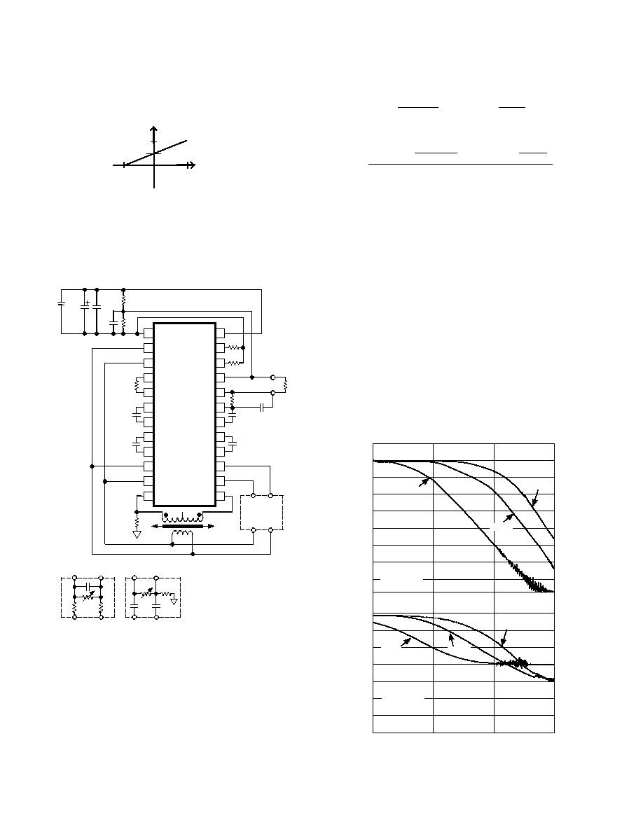
Figure 13 shows the single supply connection method.
R1
C1
C2
C3
R4
R3
13
16
15
14
24
23
22
21
20
19
18
17
12
11
10
9
8
1
2
3
4
7
6
5
AD698
–VS
EXC1
EXC2
LEV1
LEV2
FREQ1
BFILT1
BFILT2
–BIN
+BIN
–AIN
FREQ2
SIG REF
OFFSET2
OFFSET1
+VS
OUT FILT
FEEDBACK
SIG OUT
–ACOMP
AFILT2
AFILT1
+ACOMP
+AIN
C4
R2
1000pF
SIGNAL
REFERENCE
RL
VOUT
0.1F
Vps
+30V
6.8F
1M
R6
R5
C5
AB
C
D
PHASE
LAG/LEAD
NETWORK
RT
AB
CD
PHASE LEAD
RS
C
RS
RT
A
B
CD
PHASE LAG
C
PHASE LAG = Arc Tan (Hz RC);
PHASE LEAD = Arc Tan 1/(Hz RC)
WHERE R = RS// (RS + RT)
Figure 13. Interconnection Diagram for Single Supply
Operation
For single supply operation, repeat Steps 1 through 10 of the
design procedure for dual supply operation. R5, R6 and C5 are
additional component values to be determined. VOUT is mea-
sured with respect to SIGNAL REFERENCE.
10. Compute a maximum value of R5 and R6 based upon the
relationship
R5 + R6
≤ V
PS/100
A
11. The voltage drop across R5 must be greater than
2
+ 10 k
1.2V
R4
+ 2 k
+ 250 A +
VOUT
4
× R2
Volts
Therefore
R5
≥
2
+ 10 k
1.2V
R4
+ 2 k +
250
A +
VOUT
4
× R2
100
A
Ohms
Based upon the constraints of R5 + R6 (Step 10) and R5 (Step
11), select an interim value of R6.
12. Load current through RL returns to the junction of R5 and
R6, and flows back to VPS. Under maximum load condi-
tions, make sure the voltage drop across R5 is met as de-
fined in Step 11.
As a final check on the power supply voltages, verify that
the peak values of VA and VB are at least 2.5 volts less than
the voltage between +VS and –VS.
13. C5 is a bypass capacitor in the range of 0.1
F to 1 F.
Gain Phase Characteristics
To use an LVDT in a closed-loop mechanical servo application,
it is necessary to know the dynamic characteristics of the trans-
ducer and interface elements. The transducer itself is very quick
to respond once the core is moved. The dynamics arise prima-
rily from the interface electronics. Figures 14, 15 and 16 show
the frequency response of the AD698 LVDT Signal Conditioner.
Note that Figures 15 and 16 are basically the same; the differ-
ence is frequency range covered. Figure 15 shows a wider range
of mechanical input frequencies at the expense of accuracy.
FREQUENCY – Hz
0
10k
100
1k
10
0
–30
–60
–70
0
–10
–20
–50
–40
GAIN
–
dB
–360
–60
–240
–300
–420
–180
–120
PHASE
SHIFT
–
Degrees
0.1F
0.33F
2.0F
R2 = 81k
fEXC = 2.5kHz
0.1F
0.33F
2.0F
R2 = 81k
fEXC = 2.5kHz
Figure 14. Gain and Phase Characteristics vs. Frequency
(0 kHz–10 kHz)
相关PDF资料 |
PDF描述 |
|---|---|
| VE-J3B-IY-F2 | CONVERTER MOD DC/DC 95V 50W |
| MS27467T25A29PA | CONN PLUG 29POS STRAIGHT W/PINS |
| 2-227079-2 | CONN PLUG BNC 50 OHM DUAL CRIMP |
| MS27467E25A29PA | CONN PLUG 29POS STRAIGHT W/PINS |
| MS27473E24F61SB | CONN PLUG 61POS STRAIGHT W/SCKT |
相关代理商/技术参数 |
参数描述 |
|---|---|
| AD-6B | 制造商:Altas 功能描述: |
| AD6C101 | 制造商:SSOUSA 制造商全称:SSOUSA 功能描述:1 Form A Solid State Relay |
| AD6C101Q1STR | 制造商:SOLID STAT 功能描述:NEW |
| AD6C111 | 制造商:SSOUSA 制造商全称:SSOUSA 功能描述:1 Form A Solid State Relay |
| AD6C111-E | 制造商:SSOUSA 制造商全称:SSOUSA 功能描述:1 Form A Solid State Relay |
发布紧急采购,3分钟左右您将得到回复。