- 您现在的位置:买卖IC网 > PDF目录11674 > AD698SQ (Analog Devices Inc)IC LVDT SGNL COND UNVRSL 24CDIP PDF资料下载
参数资料
| 型号: | AD698SQ |
| 厂商: | Analog Devices Inc |
| 文件页数: | 5/12页 |
| 文件大小: | 0K |
| 描述: | IC LVDT SGNL COND UNVRSL 24CDIP |
| 标准包装: | 1 |
| 类型: | 信号调节器 |
| 输入类型: | 电压 |
| 输出类型: | 电压 |
| 接口: | LVDT |
| 电流 - 电源: | 15mA |
| 安装类型: | 通孔 |
| 封装/外壳: | 24-CDIP(0.600",15.24mm) |
| 供应商设备封装: | 24-CDIP |
| 包装: | 管件 |
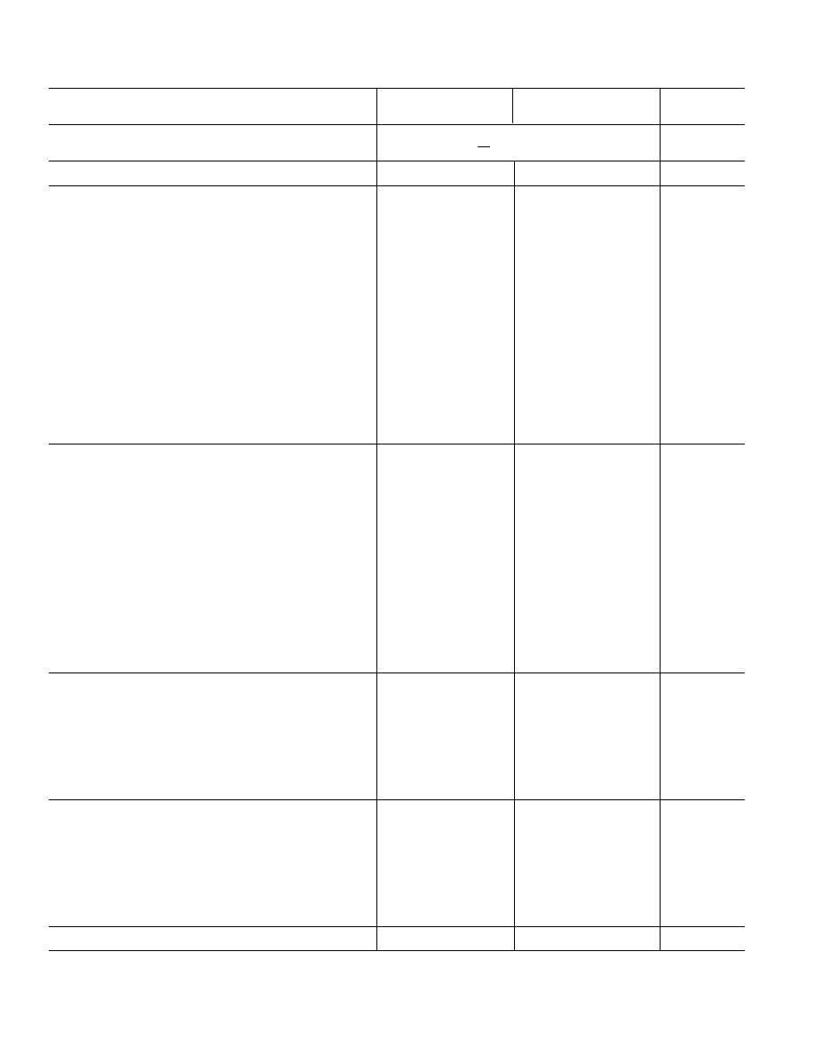
AD698–SPECIFICATIONS
REV. B
–2–
(@ TA = +25 C, VCM = 0 V, and V+, V– =
15 V dc, unless otherwise noted)
AD698SQ
AD698AP
Parameter
Min
Typ
Max
Min
Typ
Max
Unit
TRANSFER FUNCTION
1
VOUT = A
B
× 500 A × R2
V
OVERALL ERROR TMIN to TMAX
0.4
1.65
0.4
1.65
% of FS
SIGNAL OUTPUT CHARACTERISTICS
Output Voltage Range
11
V
Output Current, TMIN to TMAX
11
mA
Short Circuit Current
20
mA
Nonlinearity
2 T
MIN to TMAX
75
500
75
500
ppm of FS
Gain Error
3
0.1
1.0
0.1
1.0
% of FS
Gain Drift
20
100
20
100
ppm/
°C of FS
Output Offset
0.02
1
0.02
1
% of FS
Offset Drift
5
25
5
25
ppm/
°C of FS
Excitation Voltage Rejection
4
100
ppm/dB
Power Supply Rejection (
±12 V to ±18 V)
PSRR Gain
50
300
50
300
ppm/V
PSRR Offset
15
100
15
100
ppm/V
Common-Mode Rejection (
±3 V)
CMRR Gain
25
100
25
100
ppm/V
CMRR Offset
2
100
2
100
ppm/V
Output Ripple
5
4
mV rms
EXCITATION OUTPUT CHARACTERISTICS (@ 2.5 kHz)
Excitation Voltage Range
2.1
24
2.1
24
V rms
Excitation Voltage (Resistors Are 1% Absolute Values)
(R1 = Open)
6
1.2
2.15
1.2
2.15
V rms
(R1 = 12.7 k
)
2.6
4.35
2.6
4.35
V rms
(R1 = 487
)
14
21.2
14
21.2
V rms
Excitation Voltage TC
7
100
ppm/
°C
Output Current
30
50
30
50
mA rms
TMIN to TMAX
40
mA rms
Short Circuit Current
60
mA
DC Offset Voltage (Differential, R1 = 12.7 k
)
TMIN to TMAX
30
100
30
100
mV
Frequency
20
20 k
20
20 k
Hz
Frequency TC
200
ppm/
°C
Total Harmonic Distortion
–50
dB
SIGNAL INPUT CHARACTERISTICS
A/B Ratio Usable Full-Scale Range
0.1
0.9
0.l
0.9
Signal Voltage B Channel
0.1
3.5
0.1
3.5
V rms
Signal Voltage A Channel
0.0
3.5
0.0
3.5
V rms
Input Impedance
200
k
Input Bias Current (BIN, AIN)
1
5
1
5
A
Signal Reference Bias Current
2
10
2
10
A
Excitation Frequency
0
20 k
0
20 k
Hz
POWER SUPPLY REQUIREMENTS
Operating Range
13
36
13
36
V
Dual Supply Operation (
±10 V Output)
±13
V
Single Supply Operation
0 V to +10 V Output
17.5
V
0 V to 10 V Output
17.5
V
Current (No Load at Signal and Excitation Outputs)
12
15
12
15
mA
TMIN to TMAX
18
mA
OPERATING TEMPERATURE RANGE
–55
+125
–40
+85
°C
相关PDF资料 |
PDF描述 |
|---|---|
| VE-J3B-IY-F2 | CONVERTER MOD DC/DC 95V 50W |
| MS27467T25A29PA | CONN PLUG 29POS STRAIGHT W/PINS |
| 2-227079-2 | CONN PLUG BNC 50 OHM DUAL CRIMP |
| MS27467E25A29PA | CONN PLUG 29POS STRAIGHT W/PINS |
| MS27473E24F61SB | CONN PLUG 61POS STRAIGHT W/SCKT |
相关代理商/技术参数 |
参数描述 |
|---|---|
| AD-6B | 制造商:Altas 功能描述: |
| AD6C101 | 制造商:SSOUSA 制造商全称:SSOUSA 功能描述:1 Form A Solid State Relay |
| AD6C101Q1STR | 制造商:SOLID STAT 功能描述:NEW |
| AD6C111 | 制造商:SSOUSA 制造商全称:SSOUSA 功能描述:1 Form A Solid State Relay |
| AD6C111-E | 制造商:SSOUSA 制造商全称:SSOUSA 功能描述:1 Form A Solid State Relay |
发布紧急采购,3分钟左右您将得到回复。