- 您现在的位置:买卖IC网 > PDF目录10674 > AD7190BRUZ (Analog Devices Inc)IC ADC 2CH 24BIT W/PGA 24TSSOP PDF资料下载
参数资料
| 型号: | AD7190BRUZ |
| 厂商: | Analog Devices Inc |
| 文件页数: | 25/41页 |
| 文件大小: | 0K |
| 描述: | IC ADC 2CH 24BIT W/PGA 24TSSOP |
| 产品培训模块: | Weigh Scale Introduction |
| 设计资源: | Precision Weigh Scale Design Using AD7190 with Internal PGA (CN0102) |
| 特色产品: | AD7190 Sigma-Delta Converter |
| 标准包装: | 62 |
| 位数: | 24 |
| 采样率(每秒): | 4.8k |
| 数据接口: | DSP,MICROWIRE?,QSPI?,串行,SPI? |
| 转换器数目: | 1 |
| 电压电源: | 模拟和数字 |
| 工作温度: | -40°C ~ 105°C |
| 安装类型: | 表面贴装 |
| 封装/外壳: | 24-TSSOP(0.173",4.40mm 宽) |
| 供应商设备封装: | 24-TSSOP |
| 包装: | 管件 |
| 输入数目和类型: | 2 个差分,双极;4 个伪差分,双极 |
| 产品目录页面: | 777 (CN2011-ZH PDF) |
第1页第2页第3页第4页第5页第6页第7页第8页第9页第10页第11页第12页第13页第14页第15页第16页第17页第18页第19页第20页第21页第22页第23页第24页当前第25页第26页第27页第28页第29页第30页第31页第32页第33页第34页第35页第36页第37页第38页第39页第40页第41页
AD7190
Data Sheet
Rev. C | Page 30 of 40
Figure 3 and Figure 4 show timing diagrams for interfacing to the
AD7190, with CS being used to decode the part. Figure 3 shows
the timing for a read operation from the output shift register of
the AD7190, and Figure 4 shows the timing for a write operation
to the input shift register. It is possible to read the same word
from the data register several times even though the DOUT/RDY
line returns high after the first read operation. However, care
must be taken to ensure that the read operations have been com-
pleted before the next output update occurs. In continuous read
mode, the data register can be read only once.
The serial interface can operate in 3-wire mode by tying CS low.
In this case, the SCLK, DIN, and DOUT/RDY lines are used to
communicate with the AD7190. The end of the conversion can be
monitored using the RDY bit or pin. This scheme is suitable for
interfacing to microcontrollers.
If CS is required as a decoding signal, it can be generated from a
port pin. For microcontroller interfaces, it is recommended that
SCLK idle high between data transfers.
The AD7190 can be operated with CS used as a frame synchron-
ization signal. This scheme is useful for DSP interfaces. In this
case, the first bit (MSB) is effectively clocked out by CS because
CS normally occurs after the falling edge of SCLK in DSPs. The
SCLK can continue to run between data transfers, provided the
timing numbers are obeyed.
The serial interface can be reset by writing a series of 1s to the
DIN input. If a Logic 1 is written to the AD7190 DIN line for at
least 40 serial clock cycles, the serial interface is reset. This ensures
that the interface can be reset to a known state if the interface gets
lost due to a software error or some glitch in the system. Reset
returns the interface to the state in which it is expecting a write to
the communications register. This operation resets the contents of
all registers to their power-on values. Following a reset, the user
should allow a period of 500 s before addressing the serial
interface.
The AD7190 can be configured to continuously convert or to
perform a single conversion. See Figure 29 through Figure 31.
Single Conversion Mode
In single conversion mode, the AD7190 is placed in power-
down mode after conversions. When a single conversion is
initiated by setting MD2, MD1, and MD0 to 0, 0, 1, respectively,
in the mode register, the AD7190 powers up, performs a single
conversion, and then returns to power-down mode. The
on-chip oscillator requires 1 ms approximately to power up.
DOUT/RDY goes low to indicate the completion of a conversion.
When the data word has been read from the data register,
DOUT/RDY goes high. If CS is low, DOUT/RDY remains high
until another conversion is initiated and completed. The data
register can be read several times, if required, even when
DOUT/RDY has gone high.
If several channels are enabled, the ADC sequences through the
enabled channels and performs a conversion on each channel.
When a conversion is started, DOUT/RDY goes high and
remains high until a valid conversion is available. As soon as the
conversion is available, DOUT/RDY goes low. The ADC then
selects the next channel and begins a conversion. The user can
read the present conversion while the next conversion is being
performed. As soon as the next conversion is complete, the data
register is updated; therefore, the user has a limited period in
which to read the conversion. When the ADC has performed a
single conversion on each of the selected channels, it returns to
power-down mode.
If the DAT_STA bit in the mode register is set to 1, the contents
of the status register are output along with the conversion each
time that the data read is performed. The four LSBs of the status
register indicate the channel to which the conversion corresponds.
DIN
SCLK
DOUT/RDY
CS
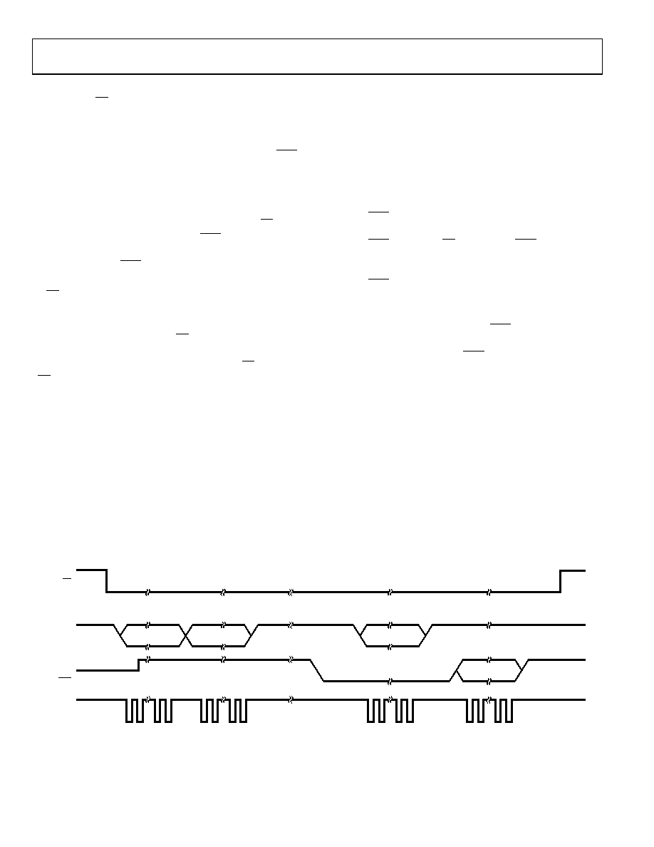
0x08
0x58
DATA
0x280060
07640-
021
Figure 29. Single Conversion
相关PDF资料 |
PDF描述 |
|---|---|
| AD7715ARZ-5 | IC ADC 16BIT SIGMA-DELTA 16-SOIC |
| AD7766BRUZ-2 | IC ADC 24BIT 32KSPS SAR 16TSSOP |
| LM2901VDG | IC COMP QUAD SGL SUPPLY 14SOIC |
| LTC1598LCG#PBF | IC A/D CONV 12BIT SRL 8CH 24SSOP |
| AD7766BRUZ-1 | IC ADC 24BIT 64KSPS SAR 16TSSOP |
相关代理商/技术参数 |
参数描述 |
|---|---|
| AD7190BRUZ | 制造商:Analog Devices 功能描述:IC, ADC, 24BIT, 4.8KSPS, TSSOP-24 |
| AD7190BRUZ-REEL | 功能描述:IC ADC 2CH 24BIT W/PGA 24TSSOP RoHS:是 类别:集成电路 (IC) >> 数据采集 - 模数转换器 系列:- 标准包装:1,000 系列:- 位数:16 采样率(每秒):45k 数据接口:串行 转换器数目:2 功率耗散(最大):315mW 电压电源:模拟和数字 工作温度:0°C ~ 70°C 安装类型:表面贴装 封装/外壳:28-SOIC(0.295",7.50mm 宽) 供应商设备封装:28-SOIC W 包装:带卷 (TR) 输入数目和类型:2 个单端,单极 |
| AD7190WBRUZ | 功能描述:24 Bit Analog to Digital Converter 2, 4 Input 1 Sigma-Delta 24-TSSOP 制造商:analog devices inc. 系列:- 包装:管件 零件状态:有效 位数:24 采样率(每秒):4.8k 输入数:2,4 输入类型:差分,个伪差分 数据接口:SPI,DSP 配置:MUX-PGA-ADC 无线电 - S/H:ADC:- A/D 转换器数:1 架构:三角积分 参考类型:外部, 内部 电压 - 电源,模拟:5V 电压 - 电源,数字:2.7 V ~ 5.25 V 特性:PGA,温度传感器 工作温度:-40°C ~ 105°C 封装/外壳:24-TSSOP(0.173",4.40mm 宽) 供应商器件封装:24-TSSOP 标准包装:1 |
| AD7190WBRUZ-RL | 制造商:Analog Devices 功能描述: |
| AD7191 | 制造商:AD 制造商全称:Analog Devices 功能描述:Pin-Programmable, Ultralow Noise, 24-Bit, Sigma-Delta ADC for Bridge Sensors |
发布紧急采购,3分钟左右您将得到回复。