参数资料
| 型号: | AD7191BRUZ |
| 厂商: | Analog Devices Inc |
| 文件页数: | 13/21页 |
| 文件大小: | 0K |
| 描述: | IC ADC 2CH 24B SD 24TSSOP |
| 产品培训模块: | Weigh Scale Introduction |
| 设计资源: | Precision Weigh Scale Design Using AD7191 with Internal PGA (CN0118) |
| 标准包装: | 62 |
| 位数: | 24 |
| 采样率(每秒): | 120 |
| 数据接口: | MICROWIRE?,QSPI?,串行,SPI? |
| 转换器数目: | 1 |
| 电压电源: | 模拟和数字 |
| 工作温度: | -40°C ~ 105°C |
| 安装类型: | 表面贴装 |
| 封装/外壳: | 24-TSSOP(0.173",4.40mm 宽) |
| 供应商设备封装: | 24-TSSOP |
| 包装: | 管件 |
| 输入数目和类型: | 2 个差分,双极 |
| 产品目录页面: | 777 (CN2011-ZH PDF) |
AD7191
Rev. A | Page 19 of 20
APPLICATIONS INFORMATION
The AD7191 provides a low-cost, high resolution analog-to-
digital function. Because the analog-to-digital function is
provided by a ∑-Δ architecture, the part is more immune to
noisy environments, making it ideal for use in sensor
measurement and industrial and process control applications.
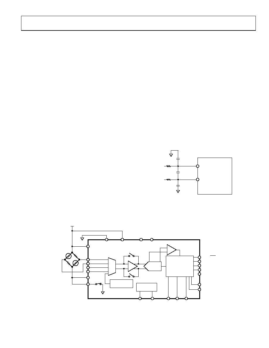
WEIGH SCALES
Figure 24 shows the AD7191 being used in a weigh scale
application. The load cell is arranged in a bridge network and
gives a differential output voltage between its OUT+ and OUT–
terminals. Assuming a 5 V excitation voltage, the full-scale
output range from the transducer is 10 mV when the sensitivity
is 2 mV/V. The excitation voltage for the bridge can be used to
directly provide the reference for the ADC because the reference
input range includes the supply voltage.
A second advantage of using the AD7191 in transducer-based
applications is that the bridge power-down switch can be fully
utilized in low power applications. The bridge power-down
switch is connected in series with the low side of the bridge. In
normal operation, the switch is closed and measurements can
be taken. In applications where power is of concern, the
AD7191 can be placed in power-down mode, thus significantly
reducing the power consumed in the application. In addition,
the bridge power-down switch is opened while in power-down
mode, thus avoiding unnecessary power consumption by the
front-end transducer. When the part is taken out of power-
down mode and the bridge power-down switch is closed, the
user should ensure that the front-end circuitry is fully settled
before attempting a read from the AD7191.
The load cell has an offset or TARE associated with it. This
TARE is the main component of the system offset (load cell plus
ADC) and is of a magnitude similar to the full-scale signal from
the load cell. For this reason, a system calibration that calibrates
the offset and full-scale error of the ADC plus the load cell is
required. A microprocessor can be used to perform the
calibrations. The offset (the conversion result from the AD7191
when no load is applied to the load cell) and the full-scale error
(the conversion result from the ADC when the maximum load
is applied to the load cell) must be determined. Subsequent
conversions from the AD7191 are then corrected using the
offset and full-scale coefficients calculated from the above
calibrations.
EMI RECOMMENDATIONS
For simplicity, the EMI filters are not included in Figure 24.
However, an R-C antialias filter should be included on each
analog input. This filter is needed because the on-chip digital
filter does not provide any rejection around MCLK/8 or
multiples of this frequency. Suitable values are a 100 Ω resistor in
series with each analog input, a 0.1 μF capacitor from AIN(+) to
AIN(), and 0.01 μF capacitors from AIN(+)/AIN() to AGND
(see Figure 23).
0.01F
100
0.1F
AD7191
100
AIN(+): AIN1 OR AIN3
AIN(–): AIN2 OR AIN4
0.01F
08
16
3-
01
8
Figure 23. External Filtering Connections
MUX
AD7191
AIN1
DOUT/RDY
SCLK
PDOWN
CHAN
CLKSEL
PGA2
REFERENCE
DETECT
PGA1
AGND
5V
IN+
OUT+
IN–
OUT–
REFIN(+)
REFIN(–)
BPDSW
AVDD
DVDD
DGND
AIN2
AIN3
AIN4
MCLK1
MCLK2
ODR2 ODR1 TEMP
TEMPERATURE
SENSOR
CLOCK
CIRCUITRY
PGA
SERIAL
INTERFACE
AND CONTROL
LOGIC
Σ-Δ
ADC
08
16
3-
0
17
Figure 24. Typical Application (Weigh Scale)
相关PDF资料 |
PDF描述 |
|---|---|
| AD7192BRUZ | IC ADC 24BIT 2CH W/PGA 24-TSSOP |
| AD7193BCPZ | IC ADC 24BIT SPI 4.8KHZ 32LFCSP |
| AD7194BCPZ | IC ADC 24BIT SPI 4.8K 32-LFCSP |
| AD7195BCPZ-RL7 | IC AFE 24BIT 4.8K 32LFSP |
| AD7225BQ | IC DAC 8BIT QUAD W/AMP 24-CDIP |
相关代理商/技术参数 |
参数描述 |
|---|---|
| AD7191BRUZ | 制造商:Analog Devices 功能描述:IC ADC 24BIT 120SPS TSSOP-24 |
| AD7191BRUZ-REEL | 功能描述:IC ADC 24BIT 2CH LN SD 24TSSOP RoHS:是 类别:集成电路 (IC) >> 数据采集 - 模数转换器 系列:- 标准包装:1,000 系列:- 位数:16 采样率(每秒):45k 数据接口:串行 转换器数目:2 功率耗散(最大):315mW 电压电源:模拟和数字 工作温度:0°C ~ 70°C 安装类型:表面贴装 封装/外壳:28-SOIC(0.295",7.50mm 宽) 供应商设备封装:28-SOIC W 包装:带卷 (TR) 输入数目和类型:2 个单端,单极 |
| AD7191KSTZ | 制造商:Analog Devices 功能描述: |
| AD7191S/0B | 制造商:Sony Nec Optiarc America 功能描述:DOUBLE DUAL INTERNAL DVDRW SATA BEZEL 20X/18X12XRAM - Bulk |
| AD7192 | 制造商:AD 制造商全称:Analog Devices 功能描述:4.8 kHz, Ultralow Noise, 24-Bit Sigma-Delta ADC with PGA |
发布紧急采购,3分钟左右您将得到回复。