参数资料
| 型号: | AD7248AQ |
| 厂商: | Analog Devices Inc |
| 文件页数: | 15/16页 |
| 文件大小: | 0K |
| 描述: | IC DAC 12BIT W/REF 24-CDIP |
| 产品培训模块: | Data Converter Fundamentals DAC Architectures |
| 标准包装: | 18 |
| 系列: | DACPORT® |
| 设置时间: | 7µs |
| 位数: | 12 |
| 数据接口: | 并联 |
| 转换器数目: | 1 |
| 电压电源: | 双 ± |
| 功率耗散(最大): | 210mW |
| 工作温度: | -40°C ~ 85°C |
| 安装类型: | 通孔 |
| 封装/外壳: | 24-CDIP(0.300",7.62mm) |
| 供应商设备封装: | 24-CDIP |
| 包装: | 管件 |
| 输出数目和类型: | 1 电压,单极;1 电压,双极 |
| 采样率(每秒): | * |
AD7245A/AD7248A
REV. B
–8–
CIRCUIT INFORMATION
D/A SECTION
The AD7245A/AD7248A contains a 12-bit voltage mode digi-
tal-to-analog converter. The output voltage from the converter
has the same positive polarity as the reference voltage allowing
single supply operation. The reference voltage for the DAC is
provided by an on-chip buried Zener diode.
The DAC consists of a highly stable, thin-film, R–2R ladder and
twelve high-speed NMOS single-pole, double-throw switches.
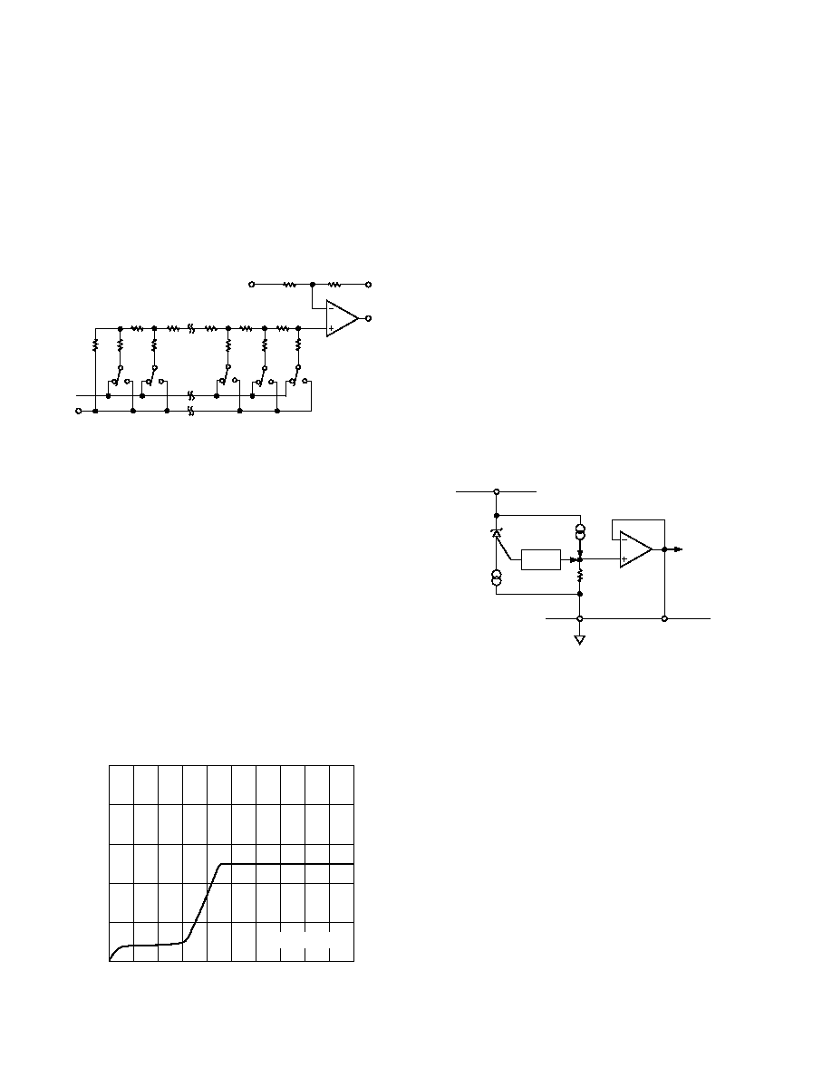
The simplified circuit diagram for this DAC is shown in Figure 1.
R
RR
R
2R
DB0
DB1
DB9
DB10
DB11
VOUT
RFB
2R
ROFS
AGND
VREF
SHOWN FOR ALL 1s ON DAC
Figure 1. D/A Simplified Circuit Diagram
The input impedance of the DAC is code dependent and can
vary from 8 k
to infinity. The input capacitance also varies
with code, typically from 50 pF to 200 pF.
OP AMP SECTION
The output of the voltage mode D/A converter is buffered by a
noninverting CMOS amplifier. The user has access to two gain
setting resistors which can be connected to allow different out-
put voltage ranges (discussed later). The buffer amplifier is
capable of developing up to 10 V across a 2 k
load to GND.
The output amplifier can be operated from a single positive
power supply by tying VSS = AGND = 0 V. The amplifier can
also be operated from dual supplies to allow a bipolar output
range of –5 V to +5 V. The advantages of having dual supplies
for the unipolar output ranges are faster settling time to voltages
near 0 V, full sink capability of 2.5 mA maintained over the entire
output range and elimination of the effects of negative offset on
the transfer characteristic (outlined previously). Figure 2 shows
the sink capability of the amplifier for single supply operation.
OUTPUT VOLTAGE – Volts
5
2
0
06
1
I SINK
–
mA
23
4
5
78
9
10
1
3
4
TA = T MIN TO T MAX
Figure 2. Typical Single Supply Sink Current vs.
Output Voltage
The small signal (200 mV p-p) bandwidth of the output buffer
amplifier is typically 1 MHz. The output noise from the ampli-
fier is low with a figure of 25 nV/
√Hz at a frequency of 1 kHz.
The broadband noise from the amplifier has a typical peak-to-
peak figure of 150
V for a 1 MHz output bandwidth. There is
no significant difference in the output noise between single and
dual supply operation.
VOLTAGE REFERENCE
The AD7245A/AD7248A contains an internal low noise buried
Zener diode reference which is trimmed for absolute accuracy
and temperature coefficient. The reference is internally connected
to the DAC. Since the DAC has a variable input impedance at
its reference input the Zener diode reference is buffered. This
buffered reference is available to the user to drive the circuitry
required for bipolar output ranges. It can be used as a reference
for other parts in the system provided it is externally buffered.
The reference will give long-term stability comparable with the
best discrete Zener reference diodes. The performance of the
AD7245A/AD7248A is specified with internal reference, and all
the testing and trimming is done with this reference. The reference
should be decoupled at the REF OUT pin and recommended
decoupling components are 10
F and 0.1 F capacitors in
series with a 10
resistor. A simplified schematic of the refer-
ence circuitry is shown in Figure 3.
VDD
TO DAC
AGND
REF OUT
IC IS TEMPERATURE
COMPENSATION CURRENT
V-TO-I
IC
Figure 3. Internal Reference
DIGITAL SECTION
The AD7245A/AD7248A digital inputs are compatible with
either TTL or 5 V CMOS levels. All data inputs are static pro-
tected MOS gates with typical input currents of less than 1 nA.
The control inputs sink higher currents (150
A max) as a result
of the fast digital interfacing. Internal input protection of all
logic inputs is achieved by on-chip distributed diodes.
The AD7245A/AD7248A features a very low digital feedthrough
figure of 10 nV-s in a 5 V output range. This is due to the volt-
age mode configuration of the DAC. Most of the impulse is
actually as a result of feedthrough across the package.
INTERFACE LOGIC INFORMATION—AD7245A
Table I shows the truth table for AD7245A operation. The part
contains two 12-bit latches, an input latch and a DAC latch.
CS
and
WR control the loading of the input latch while LDAC
controls the transfer of information from the input latch to the
DAC latch. All control signals are level triggered; and therefore,
either or both latches may be made transparent, the input latch
by keeping
CS and WR “LOW”, the DAC latch by keeping
LDAC “LOW.” Input data is latched on the rising edge of WR.
相关PDF资料 |
PDF描述 |
|---|---|
| AD7249BR | IC DAC 12BIT SRL W/REF 16-SOIC |
| AD7262BSTZ | IC ADC 2CH 12BIT PGA/COM 48LQFP |
| AD7264BCPZ | IC ADC 14BIT 2CH 1MSPS 48LFCSP |
| AD7265BSUZ-REEL7 | IC ADC 12BIT 3CHAN 1MSPS 32TQFP |
| AD7266BSUZ | IC ADC 12BIT 3CH 2MSPS 32-TQFP |
相关代理商/技术参数 |
参数描述 |
|---|---|
| AD7248ASCHIPS | 功能描述:IC DAC 12BIT W/REF 制造商:analog devices inc. 系列:* 零件状态:上次购买时间 标准包装:1 |
| AD7248ASQ/883B | 制造商:未知厂家 制造商全称:未知厂家 功能描述:12-Bit Digital-to-Analog Converter |
| AD7248ATQ | 制造商:Analog Devices 功能描述:DAC 1CH R-2R 12-BIT 20CDIP - Rail/Tube 制造商:Rochester Electronics LLC 功能描述:12-BIT DACPORT (8+4) IC - Bulk 制造商:Analog Devices 功能描述:IC DAC 12BIT W/REF 24-CDIP 制造商:Analog Devices 功能描述:CONVERTER - DAC |
| AD7248ATQ3 | 制造商:AD 制造商全称:Analog Devices 功能描述:LC2MOS 12-Bit DACPORTs |
| AD7248JN | 功能描述:IC DAC 12BIT W/REF 20-DIP RoHS:否 类别:集成电路 (IC) >> 数据采集 - 数模转换器 系列:DACPORT® 标准包装:2,400 系列:- 设置时间:- 位数:18 数据接口:串行 转换器数目:3 电压电源:模拟和数字 功率耗散(最大):- 工作温度:-40°C ~ 85°C 安装类型:表面贴装 封装/外壳:36-TFBGA 供应商设备封装:36-TFBGA 包装:带卷 (TR) 输出数目和类型:* 采样率(每秒):* |
发布紧急采购,3分钟左右您将得到回复。