参数资料
| 型号: | AD7248AQ |
| 厂商: | Analog Devices Inc |
| 文件页数: | 4/16页 |
| 文件大小: | 0K |
| 描述: | IC DAC 12BIT W/REF 24-CDIP |
| 产品培训模块: | Data Converter Fundamentals DAC Architectures |
| 标准包装: | 18 |
| 系列: | DACPORT® |
| 设置时间: | 7µs |
| 位数: | 12 |
| 数据接口: | 并联 |
| 转换器数目: | 1 |
| 电压电源: | 双 ± |
| 功率耗散(最大): | 210mW |
| 工作温度: | -40°C ~ 85°C |
| 安装类型: | 通孔 |
| 封装/外壳: | 24-CDIP(0.300",7.62mm) |
| 供应商设备封装: | 24-CDIP |
| 包装: | 管件 |
| 输出数目和类型: | 1 电压,单极;1 电压,双极 |
| 采样率(每秒): | * |
AD7245A/AD7248A
REV. B
–12–
The circuit of Figure 10 can be modified to provide a pro-
grammable current source to AGND or –VSINK (for –VSINK,
dual supplies are required on the AD7245A/AD7248A). The
AD7245A/AD7248A is configured as before. The current through
R1 is mirrored with a current mirror circuit to provide the pro-
grammable source current (see CMOS DAC Application Guide,
Publication No. G872-30-10/84, for suitable current mirror
circuit). As before the absolute value of the source current will
be affected by the
±0.2% tolerance on V
REF. In this case the perfor-
mance of the current mirror will also affect the value of the
source current.
FUNCTION GENERATOR WITH PROGRAMMABLE
FREQUENCY
Figure 11 shows how the AD7245A/AD7248A with the AD537,
voltage-to-frequency converter and the AD639, trigonometric
function generator to provide a complete function generator
with programmable frequency. The circuit provides square wave,
triwave and sine wave outputs, each output of
±10 V amplitude.
The AD7245A/AD7248A provides a programmable voltage to
the AD537 input. Since both the AD7245A/AD7248A and
AD537 are guaranteed monotonic, the output frequency will
always increase with increasing digital code. The AD537 pro-
vides a square wave output which is conditioned for
±10 V by
amplifier A1. The AD537 also provides a differential triwave
output. This is conditioned by amplifiers A2 and A3 to provide the
±1.8 V triwave required at the input of the AD639. The triwave is
further scaled by amplifier A4 to provide a
±10 V output.
Adjusting the triwave applied to the AD639 adjust the distortion
performance of the sine wave output, (10 V in configuration
shown). Amplitude, offset and symmetry of the triwave can affect
the distortion. By adjusting these, via VR1 and VR2, an output
sine wave with harmonic distortion of better than –50 dB can be
achieved at low and intermediate frequencies.
Using the capacitor value shown in Figure 11 for CF (i.e., 680 pF)
the output frequency range is 0 to 100 kHz over the digital input
code range. The step size for frequency increments is 25 Hz.
The accuracy of the output frequency is limited to 8 or 9 bits by
the AD537, but is guaranteed monotonic to 12 bits.
MICROPROCESSOR INTERFACING—AD7245
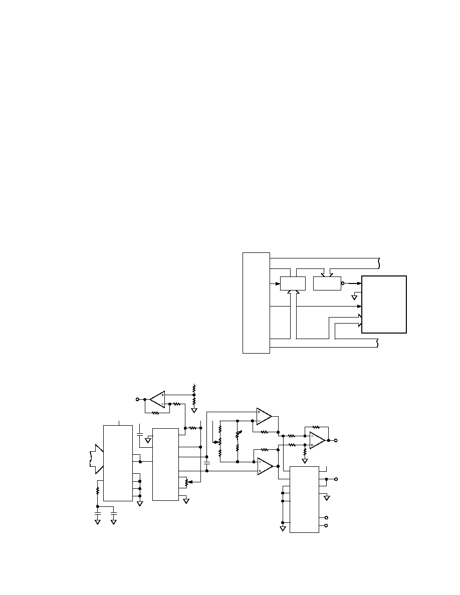
AD7245A—8086 INTERFACE
Figure 12 shows the 8086 16-bit processor interfacing to the
AD7245A. In the setup shown in Figure 12, the double buffer-
ing feature of the DAC is not used and the
LDAC input is tied
LOW. AD0–AD11 of the 16-bit data bus are connected to the
AD7245A data bus (DB0–DB11). The 12-bit word is written
to the AD7245A in one MOV instruction and the analog output
responds immediately. In this example the DAC address is
D000. A software routine for Figure 12 is given in Table V.
8086
ALE
WR
AD15
AD0
*LINEAR CIRCUITRY OMITTED FOR CLARITY
ADDRESS/DATA BUS
AD7245A*
16-BIT
LATCH
ADDRESS
DECODE
ADDRESS BUS
CS
LDAC
WR
DB11
DB0
Figure 12. AD7245A to 8086 Interface
AD537
GND
DEC
VOS
C
+VS
O/P
C
–VS
20k
+VS
+
+15V
VDD
AD7245A/
AD7248A
RFB
VOUT
ROFS
VSS
DGND
AGND
REF
OUT
10V
SQUARE
WAVE
+15V
33k
82k
+15V
4.7k
+15V
56k
5.6k
5k
VR2
4.12k
10k
VR1
3.9k
22k
A1, A2, A3, A4 – 2
AD712
CF
680pF
A3
A4
–15V
+15V
1V
SINE WAVE
20k
15k
X1
X2
U1
U2
COM
Y2
+VS
W
Z1
Z2
UP
–VS
AD639
10V
TRI WAVE
10
0.1 F10 F
+
A2
A1
Figure 11. Programmable Function Generator
Since the tolerance value on the reference voltage of the AD7245A/
AD7248A is
±0.2%, then the absolute value of ISINK can vary by
±0.2% from device to device for a fixed value of R1.
Because the input bias current of the AD7245A/AD7248A’s op
amp is only of the order of picoamps, its effect on the sink cur-
rent is negligible. Tying the ROFS input to RFB input reduces this
effect even further and prevents noise pickup which could occur
if the ROFS pin was left unconnected.
相关PDF资料 |
PDF描述 |
|---|---|
| AD7249BR | IC DAC 12BIT SRL W/REF 16-SOIC |
| AD7262BSTZ | IC ADC 2CH 12BIT PGA/COM 48LQFP |
| AD7264BCPZ | IC ADC 14BIT 2CH 1MSPS 48LFCSP |
| AD7265BSUZ-REEL7 | IC ADC 12BIT 3CHAN 1MSPS 32TQFP |
| AD7266BSUZ | IC ADC 12BIT 3CH 2MSPS 32-TQFP |
相关代理商/技术参数 |
参数描述 |
|---|---|
| AD7248ASCHIPS | 功能描述:IC DAC 12BIT W/REF 制造商:analog devices inc. 系列:* 零件状态:上次购买时间 标准包装:1 |
| AD7248ASQ/883B | 制造商:未知厂家 制造商全称:未知厂家 功能描述:12-Bit Digital-to-Analog Converter |
| AD7248ATQ | 制造商:Analog Devices 功能描述:DAC 1CH R-2R 12-BIT 20CDIP - Rail/Tube 制造商:Rochester Electronics LLC 功能描述:12-BIT DACPORT (8+4) IC - Bulk 制造商:Analog Devices 功能描述:IC DAC 12BIT W/REF 24-CDIP 制造商:Analog Devices 功能描述:CONVERTER - DAC |
| AD7248ATQ3 | 制造商:AD 制造商全称:Analog Devices 功能描述:LC2MOS 12-Bit DACPORTs |
| AD7248JN | 功能描述:IC DAC 12BIT W/REF 20-DIP RoHS:否 类别:集成电路 (IC) >> 数据采集 - 数模转换器 系列:DACPORT® 标准包装:2,400 系列:- 设置时间:- 位数:18 数据接口:串行 转换器数目:3 电压电源:模拟和数字 功率耗散(最大):- 工作温度:-40°C ~ 85°C 安装类型:表面贴装 封装/外壳:36-TFBGA 供应商设备封装:36-TFBGA 包装:带卷 (TR) 输出数目和类型:* 采样率(每秒):* |
发布紧急采购,3分钟左右您将得到回复。