参数资料
| 型号: | AD7248AQ |
| 厂商: | Analog Devices Inc |
| 文件页数: | 16/16页 |
| 文件大小: | 0K |
| 描述: | IC DAC 12BIT W/REF 24-CDIP |
| 产品培训模块: | Data Converter Fundamentals DAC Architectures |
| 标准包装: | 18 |
| 系列: | DACPORT® |
| 设置时间: | 7µs |
| 位数: | 12 |
| 数据接口: | 并联 |
| 转换器数目: | 1 |
| 电压电源: | 双 ± |
| 功率耗散(最大): | 210mW |
| 工作温度: | -40°C ~ 85°C |
| 安装类型: | 通孔 |
| 封装/外壳: | 24-CDIP(0.300",7.62mm) |
| 供应商设备封装: | 24-CDIP |
| 包装: | 管件 |
| 输出数目和类型: | 1 电压,单极;1 电压,双极 |
| 采样率(每秒): | * |
AD7245A/AD7248A
REV. B
–9–
The data held in the DAC latch determines the analog output of
the converter. Data is latched into the DAC latch on the rising
edge of
LDAC. This LDAC signal is an asynchronous signal
and is independent of
WR. This is useful in many applications.
However, in systems where the asynchronous
LDAC can occur
during a write cycle (or vice versa) care must be taken to ensure
that incorrect data is not latched through to the output. For
example, if
LDAC goes LOW while WR is “LOW,” then the
LDAC signal must stay LOW for t
7 or longer after WR goes
high to ensure correct data is latched through to the output.
Table I. AD7245A Truth Table
CLR LDAC WR
CS
Function
H
L
Both Latches are Transparent
H
X
Both Latches are Latched
H
X
H
Both Latches are Latched
H
L
Input Latches Transparent
HH
g
L
Input Latches Latched
H
L
H
DAC Latches Transparent
H
g
H
DAC Latches Latched
L
X
DAC Latches Loaded with all 0s
g
H
DAC Latches Latched with All
0s and Output Remains at
0 V or –5 V
g
L
Both Latches are Transparent
and Output Follows Input Data
H = High State, L = Low State, X = Don’t Care
The contents of the DAC latch are reset to all 0s by a low level
on the
CLR line. With both latches transparent, the CLR line
functions like a zero override with the output brought to 0 V in
the unipolar mode and –5 V in the bipolar mode for the dura-
tion of the
CLR pulse. If both latches are latched, a “LOW”
pulse on the
CLR input latches all 0s into the DAC latch and the
output remains at 0 V (or –5 V) after the
CLR line has returned
“HIGH.” The
CLR line can be used to ensure power-up to 0 V
on the AD7245A output in unipolar operation and is also use-
ful, when used as a zero override, in system calibration cycles.
Figure 4 shows the input control logic for the AD7245A and the
write cycle timing for the part is shown in Figure 5.
LDAC
CLR
WR
CS
DAC LATCH
INPUT LATCH
INPUT DATA
Figure 4. AD7245A Input Control Logic
CS
WR
LDAC
DATA
VALID
DATA
5V
0V
5V
0V
5V
0V
5V
0V
t3
t4
t5
t6
HIGH IMPEDANCE
BUS
NOTES
1. SEE TIMING SPECIFICATIONS.
2. ALL INPUT RISE AND FALL TIMES MEASURES FROM 10% TO
90% OF 5V,
tr = tf = 5ns.
3.TIMING MEASUREMENT REFERENCE LEVEL IS
VINH + V INL
2
4. IF
LDAC IS ACTIVATED WHILE WR IS LOW, LDAC MUST STAY
t1
t2
t7
LOW FOR
t7 OR LONGER AFTER WR GOES HIGH.
Figure 5. AD7245A Write Cycle Timing Diagram
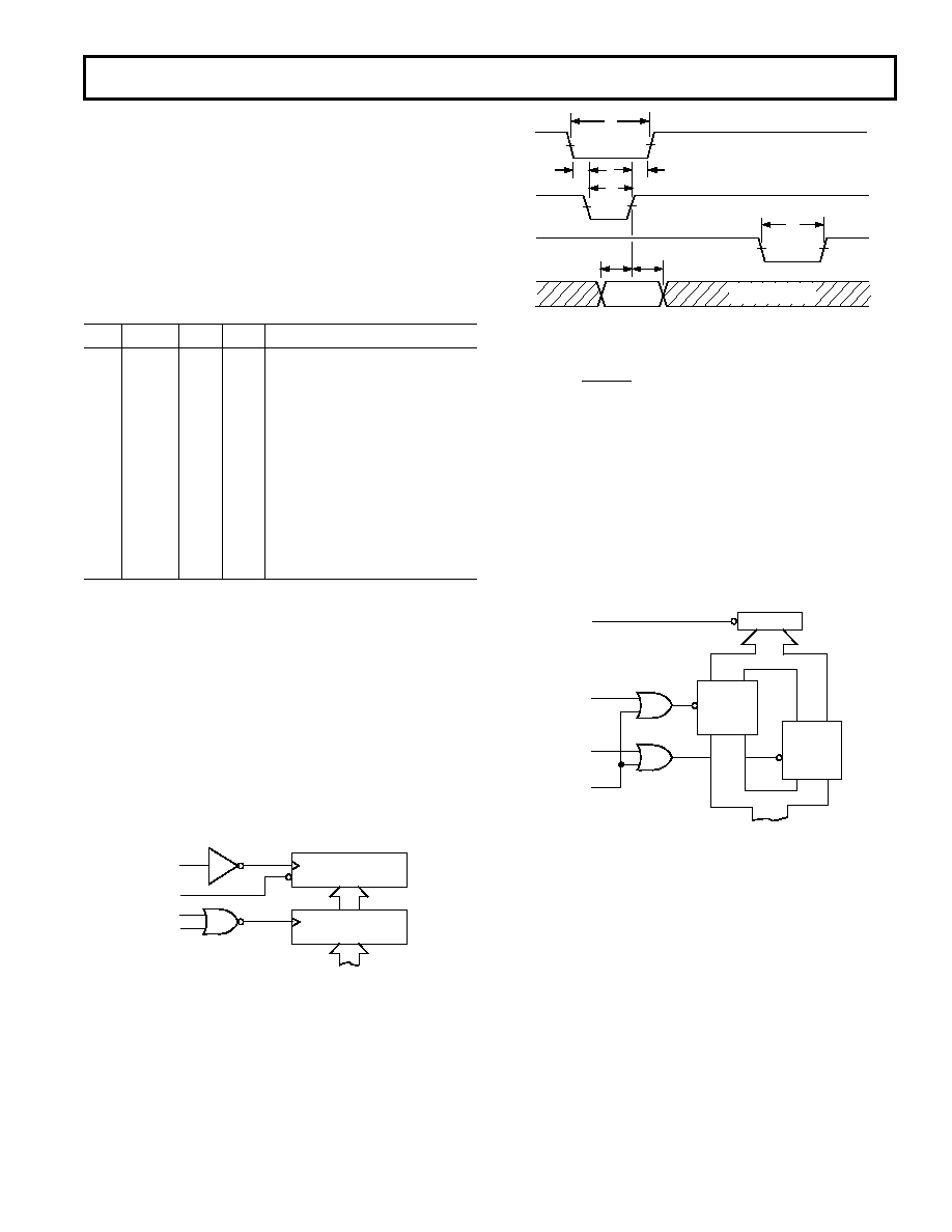
INTERFACE LOGIC INFORMATION—AD7248A
The input loading structure on the AD7248A is configured for
interfacing to microprocessors with an 8-bit wide data bus. The
part contains two 12-bit latches—an input latch and a DAC
latch. Only the data held in the DAC latch determines the ana-
log output from the converter. The truth table for AD7248A
operation is shown in Table II, while the input control logic
diagram is shown in Figure 6.
LDAC
CSMSB
CSLSB
WR
DAC LATCH
UPPER
4 BITS
OF INPUT
LATCH
LOWER
8 BITS
OF INPUT
LATCH
DB7 – DB0
12
4
8
Figure 6. AD7248A Input Control Logic
CSMSB, CSLSB and WR control the loading of data from the
external data bus to the input latch. The eight data inputs on
the AD7248A accept right justified data. This data is loaded to
the input latch in two separate write operations.
CSLSB and
WR control the loading of the lower 8-bits into the 12-bit wide
latch. The loading of the upper 4-bit nibble is controlled by
CSMSB and WR. All control inputs are level triggered, and
input data for either the lower byte or upper 4-bit nibble is
latched into the input latches on the rising edge of
WR (or
either
CSMSB or CSLSB). The order in which the data is
loaded to the input latch (i.e., lower byte or upper 4-bit nibble
first) is not important.
相关PDF资料 |
PDF描述 |
|---|---|
| AD7249BR | IC DAC 12BIT SRL W/REF 16-SOIC |
| AD7262BSTZ | IC ADC 2CH 12BIT PGA/COM 48LQFP |
| AD7264BCPZ | IC ADC 14BIT 2CH 1MSPS 48LFCSP |
| AD7265BSUZ-REEL7 | IC ADC 12BIT 3CHAN 1MSPS 32TQFP |
| AD7266BSUZ | IC ADC 12BIT 3CH 2MSPS 32-TQFP |
相关代理商/技术参数 |
参数描述 |
|---|---|
| AD7248ASCHIPS | 功能描述:IC DAC 12BIT W/REF 制造商:analog devices inc. 系列:* 零件状态:上次购买时间 标准包装:1 |
| AD7248ASQ/883B | 制造商:未知厂家 制造商全称:未知厂家 功能描述:12-Bit Digital-to-Analog Converter |
| AD7248ATQ | 制造商:Analog Devices 功能描述:DAC 1CH R-2R 12-BIT 20CDIP - Rail/Tube 制造商:Rochester Electronics LLC 功能描述:12-BIT DACPORT (8+4) IC - Bulk 制造商:Analog Devices 功能描述:IC DAC 12BIT W/REF 24-CDIP 制造商:Analog Devices 功能描述:CONVERTER - DAC |
| AD7248ATQ3 | 制造商:AD 制造商全称:Analog Devices 功能描述:LC2MOS 12-Bit DACPORTs |
| AD7248JN | 功能描述:IC DAC 12BIT W/REF 20-DIP RoHS:否 类别:集成电路 (IC) >> 数据采集 - 数模转换器 系列:DACPORT® 标准包装:2,400 系列:- 设置时间:- 位数:18 数据接口:串行 转换器数目:3 电压电源:模拟和数字 功率耗散(最大):- 工作温度:-40°C ~ 85°C 安装类型:表面贴装 封装/外壳:36-TFBGA 供应商设备封装:36-TFBGA 包装:带卷 (TR) 输出数目和类型:* 采样率(每秒):* |
发布紧急采购,3分钟左右您将得到回复。