- 您现在的位置:买卖IC网 > PDF目录10295 > AD7266BSUZ-REEL7 (Analog Devices Inc)IC ADC 12BIT 3CHAN 2MSPS 32TQFP PDF资料下载
参数资料
| 型号: | AD7266BSUZ-REEL7 |
| 厂商: | Analog Devices Inc |
| 文件页数: | 11/29页 |
| 文件大小: | 0K |
| 描述: | IC ADC 12BIT 3CHAN 2MSPS 32TQFP |
| 设计资源: | AD7266 SAR ADC in DC-Coupled Differential and Single-Ended Appls (CN0039) |
| 标准包装: | 500 |
| 位数: | 12 |
| 采样率(每秒): | 2M |
| 数据接口: | DSP,MICROWIRE?,QSPI?,串行,SPI? |
| 转换器数目: | 2 |
| 功率耗散(最大): | 33.6mW |
| 电压电源: | 模拟和数字 |
| 工作温度: | -40°C ~ 125°C |
| 安装类型: | 表面贴装 |
| 封装/外壳: | 32-TQFP |
| 供应商设备封装: | 32-TQFP(7x7) |
| 包装: | 带卷 (TR) |
| 输入数目和类型: | 12 个单端,单极;6 个差分,单极;6 个伪差分,单极 |
第1页第2页第3页第4页第5页第6页第7页第8页第9页第10页当前第11页第12页第13页第14页第15页第16页第17页第18页第19页第20页第21页第22页第23页第24页第25页第26页第27页第28页第29页
AD7266
Rev. B | Page 18 of 28
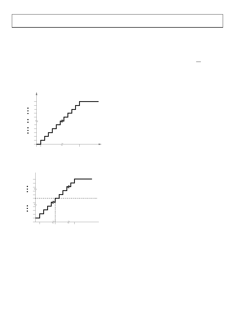
TRANSFER FUNCTIONS
The designed code transitions occur at successive integer LSB
values (1 LSB, 2 LSB, and so on). In single-ended mode, the LSB
size is VREF/4096 when the 0 V to VREF range is used, and the
LSB size is 2 × VREF/4096 when the 0 V to 2 × VREF range is used.
In differential mode, the LSB size is 2 × VREF /4096 when the 0 V
to VREF range is used, and the LSB size is 4 × VREF/4096 when the
0 V to 2 × VREF range is used. The ideal transfer characteristic
for the AD7266 when straight binary coding is output is shown
in Figure 32, and the ideal transfer characteristic for the
AD7266 when twos complement coding is output is shown in
04603-027
000...000
111...111
1LSB = VREF/4096
1LSB
VREF – 1LSB
ANALOG INPUT
ADC
CODE
0V
000...001
000...010
111...110
111...000
011...111
NOTE
1. VREF IS EITHER VREF OR 2 × VREF.
Figure 32. Straight Binary Transfer Characteristic
04603-028
100...000
011...111
1LSB = 2
× VREF/4096
+VREF – 1 LSB
–VREF + 1LSB VREF – 1LSB
ANALOG INPUT
ADC
CODE
100...001
100...010
011...110
000...001
000...000
111...111
Figure 33. Twos Complement Transfer Characteristic with
VREF ± VREF Input Range
DIGITAL INPUTS
The digital inputs applied to the AD7266 are not limited by the
maximum ratings that limit the analog inputs. Instead, the
digital inputs can be applied up to 7 V and are not restricted by
Maximum Ratings section for more information. Another
advantage of the SCLK, RANGE, A0 to A2, and CS pins not
being restricted by the VDD + 0.3 V limit is that power supply
sequencing issues are avoided. If one of these digital inputs is
applied before VDD, there is no risk of latch-up, as there would
be on the analog inputs if a signal greater than 0.3 V were
applied prior to VDD.
VDRIVE
The AD7266 also has a VDRIVE feature to control the voltage at
which the serial interface operates. VDRIVE allows the ADC to
easily interface to both 3 V and 5 V processors. For example, if
the AD7266 was operated with a VDD of 5 V, the VDRIVE pin
could be powered from a 3 V supply, allowing a large dynamic
range with low voltage digital processors. Therefore, the
AD7266 could be used with the 2 × VREF input range, with a VDD
of 5 V while still being able to interface to 3 V digital parts.
相关PDF资料 |
PDF描述 |
|---|---|
| VE-25Y-MV-S | CONVERTER MOD DC/DC 3.3V 99W |
| VE-25T-MX-S | CONVERTER MOD DC/DC 6.5V 75W |
| VE-25M-MX-S | CONVERTER MOD DC/DC 10V 75W |
| LTC1405CGN#TR | IC ADC 12BIT 5MSPS SAMPLE 28SSOP |
| LTC1420CGN#TRPBF | IC ADC 12BIT 10MSPS SAMPL 28SSOP |
相关代理商/技术参数 |
参数描述 |
|---|---|
| AD7273 | 制造商:AD 制造商全称:Analog Devices 功能描述:3MSPS,10-/12-Bit ADCs in 8-Lead TSOT |
| AD72731 | 制造商:AD 制造商全称:Analog Devices 功能描述:3 MSPS,10-/12-Bit ADCs in 8-Lead TSOT |
| AD7273BRM | 制造商:AD 制造商全称:Analog Devices 功能描述:3MSPS,10-/12-Bit ADCs in 8-Lead TSOT |
| AD7273BRMZ | 功能描述:IC ADC 10BIT 3MSPS HS LP 8MSOP RoHS:是 类别:集成电路 (IC) >> 数据采集 - 模数转换器 系列:- 其它有关文件:TSA1204 View All Specifications 标准包装:1 系列:- 位数:12 采样率(每秒):20M 数据接口:并联 转换器数目:2 功率耗散(最大):155mW 电压电源:模拟和数字 工作温度:-40°C ~ 85°C 安装类型:表面贴装 封装/外壳:48-TQFP 供应商设备封装:48-TQFP(7x7) 包装:Digi-Reel® 输入数目和类型:4 个单端,单极;2 个差分,单极 产品目录页面:1156 (CN2011-ZH PDF) 其它名称:497-5435-6 |
| AD7273BRMZ2 | 制造商:AD 制造商全称:Analog Devices 功能描述:3 MSPS,10-/12-Bit ADCs in 8-Lead TSOT |
发布紧急采购,3分钟左右您将得到回复。