- 您现在的位置:买卖IC网 > PDF目录10295 > AD7266BSUZ-REEL7 (Analog Devices Inc)IC ADC 12BIT 3CHAN 2MSPS 32TQFP PDF资料下载
参数资料
| 型号: | AD7266BSUZ-REEL7 |
| 厂商: | Analog Devices Inc |
| 文件页数: | 9/29页 |
| 文件大小: | 0K |
| 描述: | IC ADC 12BIT 3CHAN 2MSPS 32TQFP |
| 设计资源: | AD7266 SAR ADC in DC-Coupled Differential and Single-Ended Appls (CN0039) |
| 标准包装: | 500 |
| 位数: | 12 |
| 采样率(每秒): | 2M |
| 数据接口: | DSP,MICROWIRE?,QSPI?,串行,SPI? |
| 转换器数目: | 2 |
| 功率耗散(最大): | 33.6mW |
| 电压电源: | 模拟和数字 |
| 工作温度: | -40°C ~ 125°C |
| 安装类型: | 表面贴装 |
| 封装/外壳: | 32-TQFP |
| 供应商设备封装: | 32-TQFP(7x7) |
| 包装: | 带卷 (TR) |
| 输入数目和类型: | 12 个单端,单极;6 个差分,单极;6 个伪差分,单极 |
第1页第2页第3页第4页第5页第6页第7页第8页当前第9页第10页第11页第12页第13页第14页第15页第16页第17页第18页第19页第20页第21页第22页第23页第24页第25页第26页第27页第28页第29页
AD7266
Rev. B | Page 16 of 28
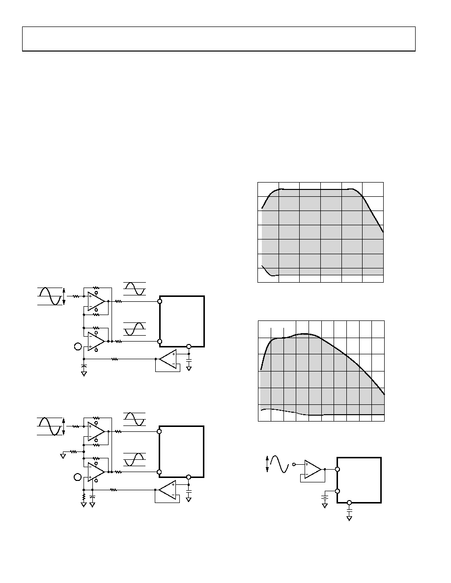
Using an Op Amp Pair
An op amp pair can be used to directly couple a differential
signal to one of the analog input pairs of the AD7266. The
show how a dual op amp can be used to convert a single-ended
signal into a differential signal for both a bipolar and unipolar
input signal, respectively.
The voltage applied to Point A sets up the common-mode
voltage. In both diagrams, it is connected in some way to the
reference, but any value in the common-mode range can be
input here to set up the common mode. The AD8022 is a
suitable dual op amp that can be used in this configuration to
provide differential drive to the AD7266.
Take care when choosing the op amp; the selection depends on
the required power supply and system performance objectives.
dc coupling applications requiring best distortion performance.
The circuit configuration shown in Figure 26 converts a
unipolar, single-ended signal into a differential signal.
The differential op amp driver circuit shown in Figure 27 is
configured to convert and level shift a single-ended, ground-
referenced (bipolar) signal to a differential signal centered at the
VREF level of the ADC.
GND
2 × VREF p-p
27
V+
V–
V+
V–
VREF
2.5V
3.75V
1.25V
2.5V
3.75V
1.25V
DCAPA/DCAPB
VIN+
AD72661
VIN–
440
220
0.47F
1ADDITIONAL PINS OMITTED FOR CLARITY.
220
10k
A
04603
-023
Figure 26. Dual Op Amp Circuit to Convert a Single-Ended Unipolar Signal
into a Differential Signal
20k
220k
2 × VREF p-p
27
V+
V–
V+
V–
GND
2.5V
3.75V
1.25V
2.5V
3.75V
1.25V
DCAPA/DCAPB
VIN+
AD72661
VIN–
440
220
0.47F
1ADDITIONAL PINS OMITTED FOR CLARITY.
220
10k
A
046
03-
024
Figure 27. Dual Op Amp Circuit to Convert a Single-Ended Bipolar Signal
into a Differential Unipolar Signal
Pseudo Differential Mode
The AD7266 can have a total of six pseudo differential pairs. In
this mode, VIN+ is connected to the signal source that must have
an amplitude of VREF (or 2 × VREF, depending on the range
chosen) to make use of the full dynamic range of the part. A dc
input is applied to the VIN pin. The voltage applied to this input
provides an offset from ground or a pseudo ground for the VIN+
input. The benefit of pseudo differential inputs is that they
separate the analog input signal ground from the ADC’s ground
allowing dc common-mode voltages to be cancelled. The typical
voltage range for the VIN pin, while in pseudo differential
mode, is shown in Figure 28 and Figure 29. Figure 30 shows a
connection diagram for pseudo differential mode.
04603-043
VREF (V)
3.0
0
0.5
1.0
1.5
2.0
2.5
V
IN–
(V
)
1.0
0.8
0.4
0.6
0.2
–0.2
0
–0.4
TA = 25°C
Figure 28. VIN- Input Voltage Range vs. VREF in
Pseudo Differential Mode with VDD = 3 V
0
460
3-
04
4
VREF (V)
5.0
0
0.5
1.0
1.5
2.0
2.5
3.0
3.5
4.0
4.5
V
IN
–(V
)
2.5
2.0
1.5
1.0
0.5
0
–0.5
TA = 25°C
Figure 29. VIN Input Voltage Range vs. VREF in
Pseudo Differential Mode with VDD = 5 V
DC INPUT
VOLTAGE
VREF
p–p
VREF
VIN+
AD72661
VIN–
0.47F
1ADDITIONAL PINS OMITTED FOR CLARITY.
04
60
3-
0
25
Figure 30. Pseudo Differential Mode Connection Diagram
相关PDF资料 |
PDF描述 |
|---|---|
| VE-25Y-MV-S | CONVERTER MOD DC/DC 3.3V 99W |
| VE-25T-MX-S | CONVERTER MOD DC/DC 6.5V 75W |
| VE-25M-MX-S | CONVERTER MOD DC/DC 10V 75W |
| LTC1405CGN#TR | IC ADC 12BIT 5MSPS SAMPLE 28SSOP |
| LTC1420CGN#TRPBF | IC ADC 12BIT 10MSPS SAMPL 28SSOP |
相关代理商/技术参数 |
参数描述 |
|---|---|
| AD7273 | 制造商:AD 制造商全称:Analog Devices 功能描述:3MSPS,10-/12-Bit ADCs in 8-Lead TSOT |
| AD72731 | 制造商:AD 制造商全称:Analog Devices 功能描述:3 MSPS,10-/12-Bit ADCs in 8-Lead TSOT |
| AD7273BRM | 制造商:AD 制造商全称:Analog Devices 功能描述:3MSPS,10-/12-Bit ADCs in 8-Lead TSOT |
| AD7273BRMZ | 功能描述:IC ADC 10BIT 3MSPS HS LP 8MSOP RoHS:是 类别:集成电路 (IC) >> 数据采集 - 模数转换器 系列:- 其它有关文件:TSA1204 View All Specifications 标准包装:1 系列:- 位数:12 采样率(每秒):20M 数据接口:并联 转换器数目:2 功率耗散(最大):155mW 电压电源:模拟和数字 工作温度:-40°C ~ 85°C 安装类型:表面贴装 封装/外壳:48-TQFP 供应商设备封装:48-TQFP(7x7) 包装:Digi-Reel® 输入数目和类型:4 个单端,单极;2 个差分,单极 产品目录页面:1156 (CN2011-ZH PDF) 其它名称:497-5435-6 |
| AD7273BRMZ2 | 制造商:AD 制造商全称:Analog Devices 功能描述:3 MSPS,10-/12-Bit ADCs in 8-Lead TSOT |
发布紧急采购,3分钟左右您将得到回复。