参数资料
| 型号: | AD7266BSUZ |
| 厂商: | Analog Devices Inc |
| 文件页数: | 10/29页 |
| 文件大小: | 0K |
| 描述: | IC ADC 12BIT 3CH 2MSPS 32-TQFP |
| 设计资源: | AD7266 SAR ADC in DC-Coupled Differential and Single-Ended Appls (CN0039) |
| 标准包装: | 1 |
| 位数: | 12 |
| 采样率(每秒): | 2M |
| 数据接口: | DSP,MICROWIRE?,QSPI?,串行,SPI? |
| 转换器数目: | 2 |
| 功率耗散(最大): | 33.6mW |
| 电压电源: | 模拟和数字 |
| 工作温度: | -40°C ~ 125°C |
| 安装类型: | 表面贴装 |
| 封装/外壳: | 32-TQFP |
| 供应商设备封装: | 32-TQFP(7x7) |
| 包装: | 托盘 |
| 输入数目和类型: | 12 个单端,单极;6 个差分,单极;6 个伪差分,单极 |
| 产品目录页面: | 777 (CN2011-ZH PDF) |
第1页第2页第3页第4页第5页第6页第7页第8页第9页当前第10页第11页第12页第13页第14页第15页第16页第17页第18页第19页第20页第21页第22页第23页第24页第25页第26页第27页第28页第29页
AD7266
Rev. B | Page 17 of 28
The channels used for simultaneous conversions are selected via
the multiplexer address input pins, A0 to A2. The logic states of
these pins also need to be established prior to the acquisition
time; however, they may change during the conversion time
provided the mode is not changed. If the mode is changed from
fully differential to pseudo differential, for example, then the
acquisition time would start again from this point. The selected
input channels are decoded as shown in Table 6.
ANALOG INPUT SELECTION
The analog inputs of the AD7266 can be configured as single-
ended or true differential via the SGL/DIFF logic pin, as shown
in
. If this pin is tied to a logic low, the analog input
channels to each on-chip ADC are set up as three true
differential pairs. If this pin is at logic high, the analog input
channels to each on-chip ADC are set up as six single-ended
analog inputs. The required logic level on this pin needs to be
established prior to the acquisition time and remain unchanged
during the conversion time until the track-and-hold has returned
to track. The track-and-hold returns to track on the 13th rising
edge of SCLK after the
CS falling edge (see
). If the
level on this pin is changed, it will be recognized by the
AD7266; therefore, it is necessary to keep the same logic level
during acquisition and conversion to avoid corrupting the
conversion in progress.
The analog input range of the AD7266 can be selected as 0 V to
VREF or 0 V to 2 × VREF via the RANGE pin. This selection is
made in a similar fashion to that of the SGL/DIFF pin by setting
the logic state of the RANGE pin a time tacq prior to the falling
edge of CS. Subsequent to this, the logic level on this pin can be
altered after the third falling edge of SCLK. If this pin is tied to a
logic low, the analog input range selected is 0 V to VREF. If this
pin is tied to a logic high, the analog input range selected is 0 V
to 2 × VREF.
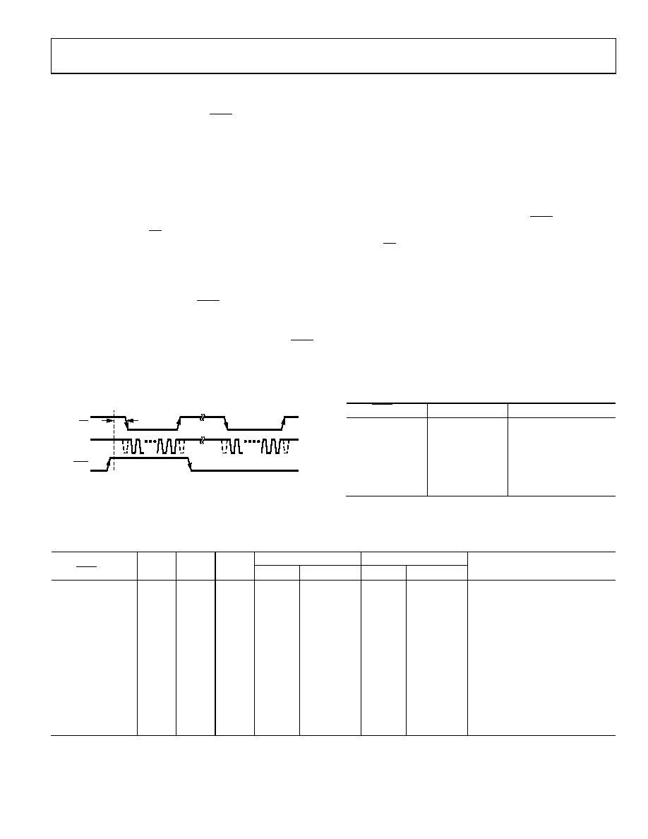
For example, in Figure 31 the SGL/DIFF pin is set at logic high
for the duration of both the acquisition and conversion times so
the analog inputs are configured as single ended for that
conversion (Sampling Point A). The logic level of the SGL/DIFF
changed to low after the track-and-hold returned to track and
prior to the required acquisition time for the next sampling
instant at Point B; therefore, the analog inputs are configured as
differential for that conversion.
OUTPUT CODING
The AD7266 output coding is set to either twos complement or
straight binary, depending on which analog input configuration
is selected for a conversion. Table 5 shows which output coding
scheme is used for each possible analog input configuration.
Table 5. AD7266 Output Coding
SGL/DIFF
Range
Output Coding
DIFF
SCLK
CS
114
14
1
A
SGL/DIFF
B
tACQ
04603-026
0 V to VREF
Twos complement
DIFF
0 V to 2 × VREF
Twos complement
SGL
0 V to VREF
Straight binary
SGL
0 V to 2 × VREF
Twos complement
PSEUDO DIFF
0 V to VREF
Straight binary
PSEUDO DIFF
Figure 31. Selecting Differential or Single-Ended Configuration
0 V to 2 × VREF
Twos complement
Table 6. Analog Input Type and Channel Selection
ADC A
ADC B
SGL/DIFF
A2
A1
A0
VIN+
VIN
VIN+
VIN
Comment
1
0
VA1
AGND
VB1
AGND
Single ended
1
0
1
VA2
AGND
VB2
AGND
Single ended
1
0
1
0
VA3
AGND
VB3
AGND
Single ended
1
0
1
VA4
AGND
VB4
AGND
Single ended
1
0
VA5
AGND
VB5
AGND
Single ended
1
0
1
VA6
AGND
VB6
AGND
Single ended
0
VA1
VA2
VB1
VB2
Fully differential
0
1
VA1
VA2
VB1
VB2
Pseudo differential
0
1
0
VA3
VA4
VB3
VB4
Fully differential
0
1
VA3
VA4
VB3
VB4
Pseudo differential
0
1
0
VA5
VA6
VB5
VB6
Fully differential
0
1
0
1
VA5
VA6
VB5
VB6
Pseudo differential
相关PDF资料 |
PDF描述 |
|---|---|
| AD7274BRM | IC ADC 12BIT 3MSPS HS LP 8MSOP |
| AD7276BRM | IC ADC 12BIT 3MSPS HS LP 8MSOP |
| AD7291BCPZ-RL7 | IC ADC I2C/SRL 22.22K 20LFCSP |
| AD7298-1BCPZ-RL | IC ADC 10BIT SPI/SRL 8CH 20LFCSP |
| AD7298BCPZ-RL7 | IC ADC 10BIT SPI/SRL 8CH 20LFCSP |
相关代理商/技术参数 |
参数描述 |
|---|---|
| AD7266BSUZ-REEL | 功能描述:IC ADC 12BIT 3CHAN 2MSPS 32TQFP RoHS:是 类别:集成电路 (IC) >> 数据采集 - 模数转换器 系列:- 标准包装:1,000 系列:- 位数:16 采样率(每秒):45k 数据接口:串行 转换器数目:2 功率耗散(最大):315mW 电压电源:模拟和数字 工作温度:0°C ~ 70°C 安装类型:表面贴装 封装/外壳:28-SOIC(0.295",7.50mm 宽) 供应商设备封装:28-SOIC W 包装:带卷 (TR) 输入数目和类型:2 个单端,单极 |
| AD7266BSUZ-REEL7 | 功能描述:IC ADC 12BIT 3CHAN 2MSPS 32TQFP RoHS:是 类别:集成电路 (IC) >> 数据采集 - 模数转换器 系列:- 标准包装:1,000 系列:- 位数:16 采样率(每秒):45k 数据接口:串行 转换器数目:2 功率耗散(最大):315mW 电压电源:模拟和数字 工作温度:0°C ~ 70°C 安装类型:表面贴装 封装/外壳:28-SOIC(0.295",7.50mm 宽) 供应商设备封装:28-SOIC W 包装:带卷 (TR) 输入数目和类型:2 个单端,单极 |
| AD7273 | 制造商:AD 制造商全称:Analog Devices 功能描述:3MSPS,10-/12-Bit ADCs in 8-Lead TSOT |
| AD72731 | 制造商:AD 制造商全称:Analog Devices 功能描述:3 MSPS,10-/12-Bit ADCs in 8-Lead TSOT |
| AD7273BRM | 制造商:AD 制造商全称:Analog Devices 功能描述:3MSPS,10-/12-Bit ADCs in 8-Lead TSOT |
发布紧急采购,3分钟左右您将得到回复。