- 您现在的位置:买卖IC网 > PDF目录1980 > AD7298-1BCPZ-RL (Analog Devices Inc)IC ADC 10BIT SPI/SRL 8CH 20LFCSP PDF资料下载
参数资料
| 型号: | AD7298-1BCPZ-RL |
| 厂商: | Analog Devices Inc |
| 文件页数: | 6/25页 |
| 文件大小: | 0K |
| 描述: | IC ADC 10BIT SPI/SRL 8CH 20LFCSP |
| 标准包装: | 1 |
| 位数: | 10 |
| 采样率(每秒): | 1M |
| 数据接口: | DSP,串行,SPI? |
| 转换器数目: | 1 |
| 功率耗散(最大): | 23mW |
| 电压电源: | 单电源 |
| 工作温度: | -40°C ~ 125°C |
| 安装类型: | 表面贴装 |
| 封装/外壳: | 20-WFQFN 裸露焊盘,CSP |
| 供应商设备封装: | 20-LFCSP-WQ(4x4) |
| 包装: | 标准包装 |
| 输入数目和类型: | 8 个单端,单极 |
| 其它名称: | AD7298-1BCPZ-RLDKR |
AD7298-1
Rev. A | Page 13 of 24
CIRCUIT INFORMATION
The AD7298-1 is a high speed, 8-channel, 10-bit ADC. The part
can be operated from a 2.8 V to 3.6 V supply and is capable of
throughput rates of 1 MSPS per analog input channel.
The AD7298-1 provides the user with an on-chip, track-and-hold
ADC and a serial interface housed in a 20-lead LFCSP. The
AD7298-1 has eight, single-ended input channels with channel
repeat functionality, which allows the user to select a channel
sequence through which the ADC can cycle with each consecutive
CS falling edge. The serial clock input accesses data from the
part, controls the transfer of data written to the ADC, and
provides the clock source for the successive approximation
ADC. The analog input range for the AD7928-1 is 0 V to VREF.
The AD7298-1 operates with one cycle latency, which means
that the conversion result is available in the serial transfer
following the cycle in which the conversion is performed.
The AD7298-1 provides flexible power management options to
allow the user to achieve the best power performance for a given
throughput rate. These options are selected by programming
the partial power-down bit, PPD, in the control register and
using the PD/RST pin.
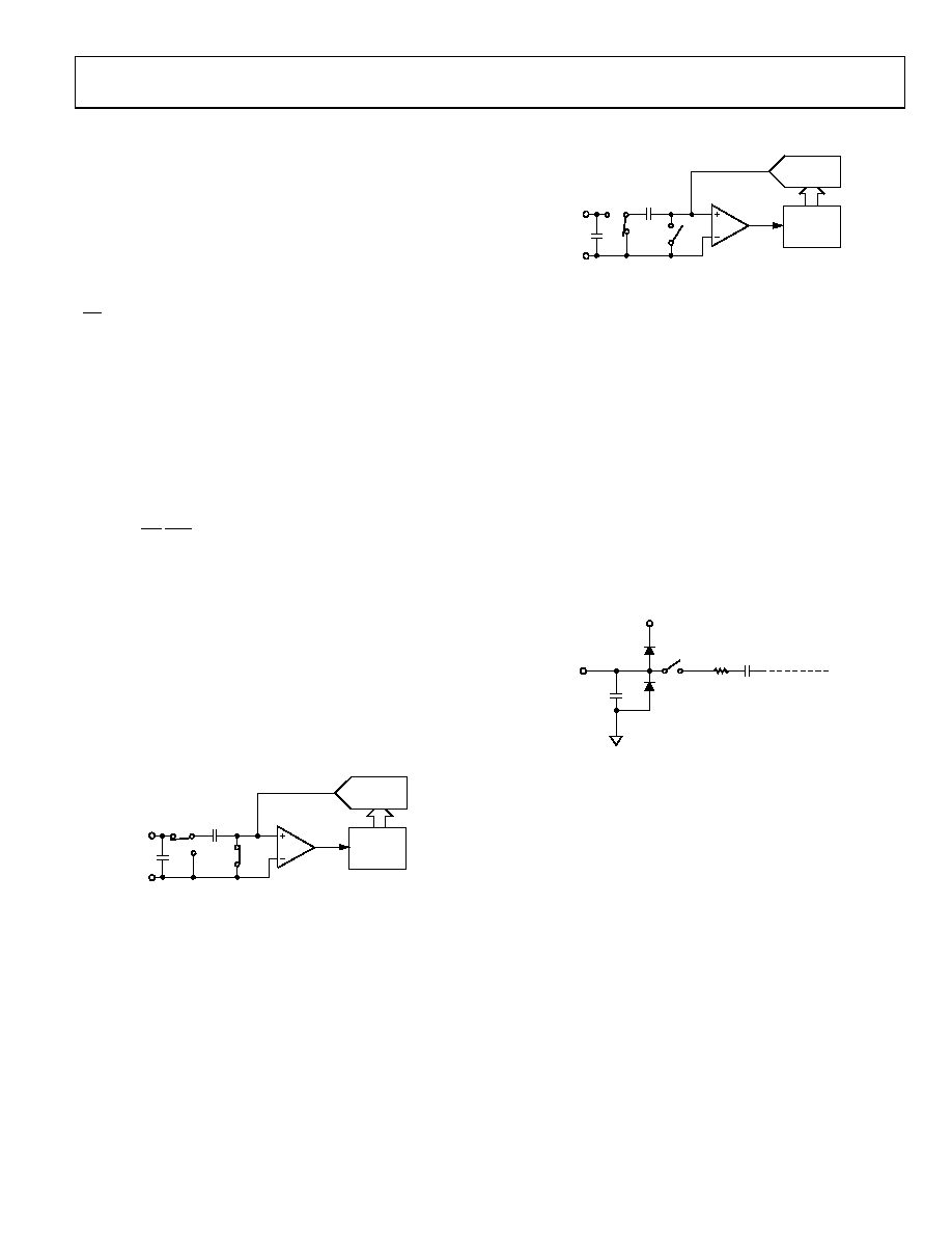
CONVERTER OPERATION
The AD7298-1 is a 10-bit successive approximation ADC based
around a capacitive DAC. Figure 19 and Figure 20 show simplified
schematics of the ADC. The ADC is comprised of control logic,
SAR, and a capacitive DAC that are used to add and subtract
fixed amounts of charge from the sampling capacitor to bring
the comparator back into a balanced condition. Figure 19 shows
the ADC during its acquisition phase. SW2 is closed and SW1 is
in Position A. The comparator is held in a balanced condition
and the sampling capacitor acquires the signal on the selected
VIN channel.
CONTROL
LOGIC
CAPACITIVE
DAC
VIN
A
B
SW1
SW2
GND1
COMPARATOR
08
75
4-
0
04
Figure 19. ADC Acquisition Phase
When the ADC starts a conversion (see Figure 20), SW2 opens
and SW1 moves to Position B, causing the comparator to become
unbalanced. The control logic and the capacitive DAC are used to
add and subtract fixed amounts of charge to bring the comparator
back into a balanced condition. When the comparator is
rebalanced, the conversion is complete. The control logic
generates the ADC output code. Figure 22 shows the transfer
function of the ADC.
CONTROL
LOGIC
CAPACITIVE
DAC
VIN
A
B
SW1
SW2
GND1
COMPARATOR
09
32
1-
0
05
Figure 20. ADC Conversion Phase
ANALOG INPUT
Figure 21 shows an equivalent circuit of the analog input structure
of the AD7298-1. The two diodes, D1 and D2, provide ESD
protection for the analog inputs. Care must be taken to ensure
that the analog input signal never exceeds the internally generated
LDO voltage of 2.5 V (DCAP) by more than 300 mV. This causes
the diodes to become forward-biased and to start conducting
current into the substrate. The maximum current these diodes
can conduct without causing irreversible damage to the part is
10 mA. Capacitor C1, in Figure 21, is typically about 8 pF and
can primarily be attributed to pin capacitance. The R1 resistor is
a lumped component made up of the on resistance of a switch
(track-and-hold switch) and includes the on resistance of the
input multiplexer. The total resistance is typically about 155 Ω.
The capacitor, C2, is the ADC sampling capacitor and has a
capacitance of 34 pF typically.
C1
pF
C2
pF
R1
D2
CONVERSION PHASE: SWITCH OPEN
TRACK PHASE: SWITCH CLOSED
D1
DCAP (2.5V)
VIN
0
932
1-
00
6
Figure 21. Equivalent Analog Input Circuit
For ac applications, removing high frequency components from
the analog input signal is recommended by using an RC low-pass
filter on the relevant analog input pin. In applications where
harmonic distortion and signal-to-noise ratios are critical, the
analog input should be driven from a low impedance source. Large
source impedances significantly affect the ac performance of the
ADC. This may necessitate the use of an input buffer amplifier.
The choice of the op amp is a function of the particular application
performance criteria.
相关PDF资料 |
PDF描述 |
|---|---|
| AD7298BCPZ-RL7 | IC ADC 10BIT SPI/SRL 8CH 20LFCSP |
| AD7302BRUZ-REEL7 | IC DAC 8BIT DUAL R-R 20-TSSOP |
| AD7303BRM | IC DAC 8BIT DUAL R-R 8-MSOP |
| AD7305BRU | IC DAC 8BIT QUAD R-R 20-TSSOP |
| AD7321BRUZ-REEL7 | IC ADC 12BIT+ SAR 2CHAN 14TSSOP |
相关代理商/技术参数 |
参数描述 |
|---|---|
| AD7298BCPZ | 功能描述:IC ADC 12BIT SPI/SRL 1M 20LFCSP RoHS:是 类别:集成电路 (IC) >> 数据采集 - 模数转换器 系列:- 标准包装:1 系列:microPOWER™ 位数:8 采样率(每秒):1M 数据接口:串行,SPI? 转换器数目:1 功率耗散(最大):- 电压电源:模拟和数字 工作温度:-40°C ~ 125°C 安装类型:表面贴装 封装/外壳:24-VFQFN 裸露焊盘 供应商设备封装:24-VQFN 裸露焊盘(4x4) 包装:Digi-Reel® 输入数目和类型:8 个单端,单极 产品目录页面:892 (CN2011-ZH PDF) 其它名称:296-25851-6 |
| AD7298BCPZ-RL7 | 功能描述:IC ADC 10BIT SPI/SRL 8CH 20LFCSP RoHS:是 类别:集成电路 (IC) >> 数据采集 - 模数转换器 系列:- 标准包装:1,000 系列:- 位数:16 采样率(每秒):45k 数据接口:串行 转换器数目:2 功率耗散(最大):315mW 电压电源:模拟和数字 工作温度:0°C ~ 70°C 安装类型:表面贴装 封装/外壳:28-SOIC(0.295",7.50mm 宽) 供应商设备封装:28-SOIC W 包装:带卷 (TR) 输入数目和类型:2 个单端,单极 |
| AD73 | 制造商:Distributed By MCM 功能描述:REFRIGERATR DOOR GASKET DIRECT |
| AD7302 | 制造商:AD 制造商全称:Analog Devices 功能描述:2.7 V to 5.5 V, Parallel Input Dual Voltage Output 8-Bit DAC |
| AD7302BN | 功能描述:IC DAC 8BIT DUAL R-R 20-DIP RoHS:否 类别:集成电路 (IC) >> 数据采集 - 数模转换器 系列:- 标准包装:2,400 系列:- 设置时间:- 位数:18 数据接口:串行 转换器数目:3 电压电源:模拟和数字 功率耗散(最大):- 工作温度:-40°C ~ 85°C 安装类型:表面贴装 封装/外壳:36-TFBGA 供应商设备封装:36-TFBGA 包装:带卷 (TR) 输出数目和类型:* 采样率(每秒):* |
发布紧急采购,3分钟左右您将得到回复。