- 您现在的位置:买卖IC网 > PDF目录1980 > AD7298BCPZ-RL7 (Analog Devices Inc)IC ADC 10BIT SPI/SRL 8CH 20LFCSP PDF资料下载
参数资料
| 型号: | AD7298BCPZ-RL7 |
| 厂商: | Analog Devices Inc |
| 文件页数: | 24/25页 |
| 文件大小: | 0K |
| 描述: | IC ADC 10BIT SPI/SRL 8CH 20LFCSP |
| 标准包装: | 1 |
| 位数: | 12 |
| 采样率(每秒): | 1M |
| 数据接口: | DSP,串行,SPI? |
| 转换器数目: | 1 |
| 功率耗散(最大): | 22.7mW |
| 电压电源: | 单电源 |
| 工作温度: | -40°C ~ 125°C |
| 安装类型: | 表面贴装 |
| 封装/外壳: | 20-WFQFN 裸露焊盘,CSP |
| 供应商设备封装: | 20-LFCSP-WQ(4x4) |
| 包装: | 标准包装 |
| 输入数目和类型: | 8 个单端,单极 |
| 其它名称: | AD7298BCPZ-RL7DKR |
AD7298
Rev. B | Page 7 of 24
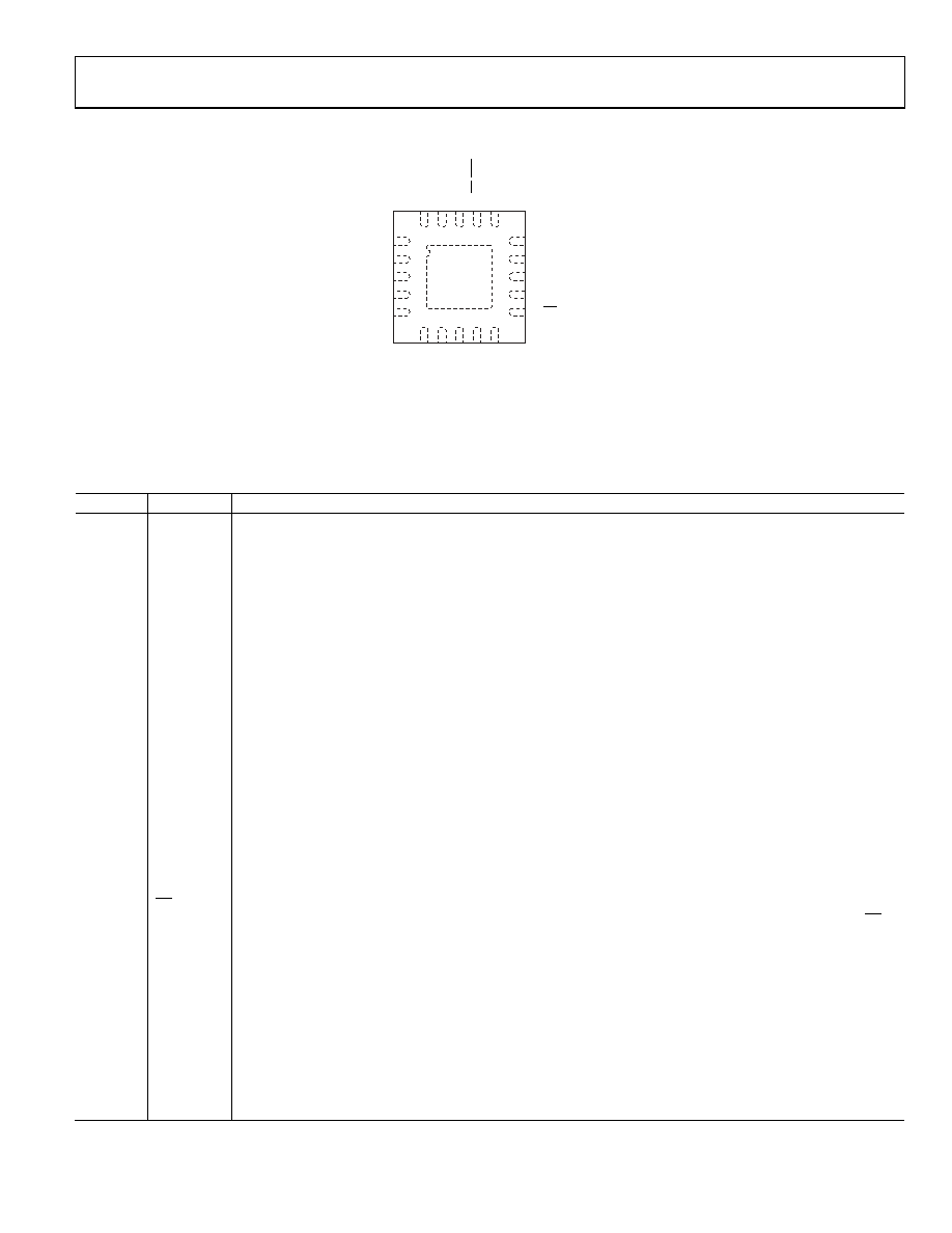
PIN CONFIGURATION AND FUNCTION DESCRIPTION
14
13
12
1
3
4
DOUT
15
SCLK
DIN
TSENSE_BUSY
11
CS
VIN3
VIN5
2
VIN4
VIN6
5
VIN7
7
V
R
E
F
6
G
N
D
1
8
D
C
A
P
9
G
N
D
10
V
D
19
V
IN
1
20
V
IN
2
18
V
IN
0
17
P
D
/R
S
T
16
V
D
R
IV
E
AD7298
TOP VIEW
(Not to Scale)
08
75
4-
00
3
NOTES
1. THE EXPOSED METAL PADDLE ON THE BOTTOM
OF THE LFCSP PACKAGE SHOULD BE SOLDERED
TO PCB GROUND FOR PROPER FUNCTIONALITY
AND HEAT DISSIPATION.
Figure 2. Pin Configuration
Table 5. Pin Function Descriptions
Pin No.
Mnemonic
Description
1 to 5,
18 to 20
VIN3, VIN4,
VIN5, VIN6,
VIN7, VIN0,
VIN1, VIN2
Analog Inputs. The AD7298 has eight single-ended analog inputs that are multiplexed into the on-chip track-
and-hold. Each input channel can accept analog inputs from 0 V to 2.5 V. Any unused input channels should be
connected to GND1 to avoid noise pickup.
6
GND1
Ground. Ground reference point for the internal reference circuitry on the AD7298. The external reference signals
and all analog input signals should be referred to this GND1 voltage. The GND1 pin should be connected to the
GND plane of a system. All ground pins should ideally be at the same potential and must not be more than 0.3 V
apart, even on a transient basis. The VREF pin should be decoupled to this ground pin via a 10 μF decoupling
capacitor.
7
VREF
Internal Reference/External Reference Supply. The nominal internal reference voltage of 2.5 V appears at this pin.
Provided the output is buffered, the on-chip reference can be taken from this pin and applied externally to the
rest of a system. Decoupling capacitors should be connected to this pin to decouple the reference buffer. For
best performance, it is recommended to use a 10 μF decoupling capacitor on this pin to GND1. The internal
reference can be disabled and an external reference supplied to this pin, if required. The input voltage range for
the external reference is 2.0 V to 2.5 V.
8
DCAP
Decoupling Capacitor Pin. Decoupling capacitors (1 μF recommended) are connected to this pin to decouple the
internal LDO.
9
GND
Ground. Ground reference point for all analog and digital circuitry on the AD7298. The GND pin should be
connected to the ground plane of the system. All ground pins should ideally be at the same potential and must
not be more than 0.3 V apart, even on a transient basis. Both DCAP and VDD pins should be decoupled to this
GND pin.
10
VDD
Supply Voltage, 2.8 V to 3.6 V. This supply should be decoupled to GND with 10 μF and 100 nF decoupling
capacitors.
11
CS
Chip Select, Active Low Logic Input. This pin is edge triggered on the falling edge of this input, the track-and-
hold goes into hold mode, and a conversion is initiated. This input also frames the serial data transfer. When CS is
low, the output bus is enabled, and the conversion result becomes available on the DOUT output.
12
TSENSE_BUSY
Busy Output. This pin transitions high when a temperature sensor conversion starts and remains high until the
conversion completes.
13
DIN
Data In, Logic input. Data to be written to the AD7298 control register is provided on this input and is clocked
into the register on the falling edge of SCLK.
14
DOUT
Serial Data Output. The conversion result from the AD7298 is provided on this output as a serial data stream. The
bits are clocked out on the falling edge of the SCLK input. The data stream from the AD7298 consists of four
address bits indicating which channel the conversion result corresponds to, followed by the 12 bits of conversion
data (MSB first). The output coding is straight binary for the voltage channels and twos complement for the
temperature sensor result.
15
SCLK
Serial Clock, Logic Input. A serial clock input provides the SCLK for accessing the data from the AD7298.
相关PDF资料 |
PDF描述 |
|---|---|
| AD7302BRUZ-REEL7 | IC DAC 8BIT DUAL R-R 20-TSSOP |
| AD7303BRM | IC DAC 8BIT DUAL R-R 8-MSOP |
| AD7305BRU | IC DAC 8BIT QUAD R-R 20-TSSOP |
| AD7321BRUZ-REEL7 | IC ADC 12BIT+ SAR 2CHAN 14TSSOP |
| AD7322BRUZ-REEL7 | IC ADC 12BIT+ SAR 2CHAN 14TSSOP |
相关代理商/技术参数 |
参数描述 |
|---|---|
| AD73 | 制造商:Distributed By MCM 功能描述:REFRIGERATR DOOR GASKET DIRECT |
| AD7302 | 制造商:AD 制造商全称:Analog Devices 功能描述:2.7 V to 5.5 V, Parallel Input Dual Voltage Output 8-Bit DAC |
| AD7302BN | 功能描述:IC DAC 8BIT DUAL R-R 20-DIP RoHS:否 类别:集成电路 (IC) >> 数据采集 - 数模转换器 系列:- 标准包装:2,400 系列:- 设置时间:- 位数:18 数据接口:串行 转换器数目:3 电压电源:模拟和数字 功率耗散(最大):- 工作温度:-40°C ~ 85°C 安装类型:表面贴装 封装/外壳:36-TFBGA 供应商设备封装:36-TFBGA 包装:带卷 (TR) 输出数目和类型:* 采样率(每秒):* |
| AD7302BNZ | 功能描述:IC DAC 8BIT DUAL R-R 20-DIP RoHS:是 类别:集成电路 (IC) >> 数据采集 - 数模转换器 系列:- 产品培训模块:Lead (SnPb) Finish for COTS Obsolescence Mitigation Program 标准包装:50 系列:- 设置时间:4µs 位数:12 数据接口:串行 转换器数目:2 电压电源:单电源 功率耗散(最大):- 工作温度:-40°C ~ 85°C 安装类型:表面贴装 封装/外壳:8-TSSOP,8-MSOP(0.118",3.00mm 宽) 供应商设备封装:8-uMAX 包装:管件 输出数目和类型:2 电压,单极 采样率(每秒):* 产品目录页面:1398 (CN2011-ZH PDF) |
| AD7302BR | 功能描述:IC DAC 8BIT DUAL 2.7V 20-SOIC RoHS:否 类别:集成电路 (IC) >> 数据采集 - 数模转换器 系列:- 标准包装:2,400 系列:- 设置时间:- 位数:18 数据接口:串行 转换器数目:3 电压电源:模拟和数字 功率耗散(最大):- 工作温度:-40°C ~ 85°C 安装类型:表面贴装 封装/外壳:36-TFBGA 供应商设备封装:36-TFBGA 包装:带卷 (TR) 输出数目和类型:* 采样率(每秒):* |
发布紧急采购,3分钟左右您将得到回复。