- 您现在的位置:买卖IC网 > PDF目录10681 > AD7298BCPZ (Analog Devices Inc)IC ADC 12BIT SPI/SRL 1M 20LFCSP PDF资料下载
参数资料
| 型号: | AD7298BCPZ |
| 厂商: | Analog Devices Inc |
| 文件页数: | 15/25页 |
| 文件大小: | 0K |
| 描述: | IC ADC 12BIT SPI/SRL 1M 20LFCSP |
| 特色产品: | AD7298 ADC with Temperature Sensor |
| 标准包装: | 1 |
| 位数: | 12 |
| 采样率(每秒): | 1M |
| 数据接口: | DSP,串行,SPI? |
| 转换器数目: | 1 |
| 功率耗散(最大): | 22.7mW |
| 电压电源: | 单电源 |
| 工作温度: | -40°C ~ 125°C |
| 安装类型: | 表面贴装 |
| 封装/外壳: | 20-WFQFN 裸露焊盘,CSP |
| 供应商设备封装: | 20-LFCSP-WQ(4x4) |
| 包装: | 托盘 |
| 输入数目和类型: | 8 个单端,单极 |
AD7298
Rev. B | Page 21 of 24
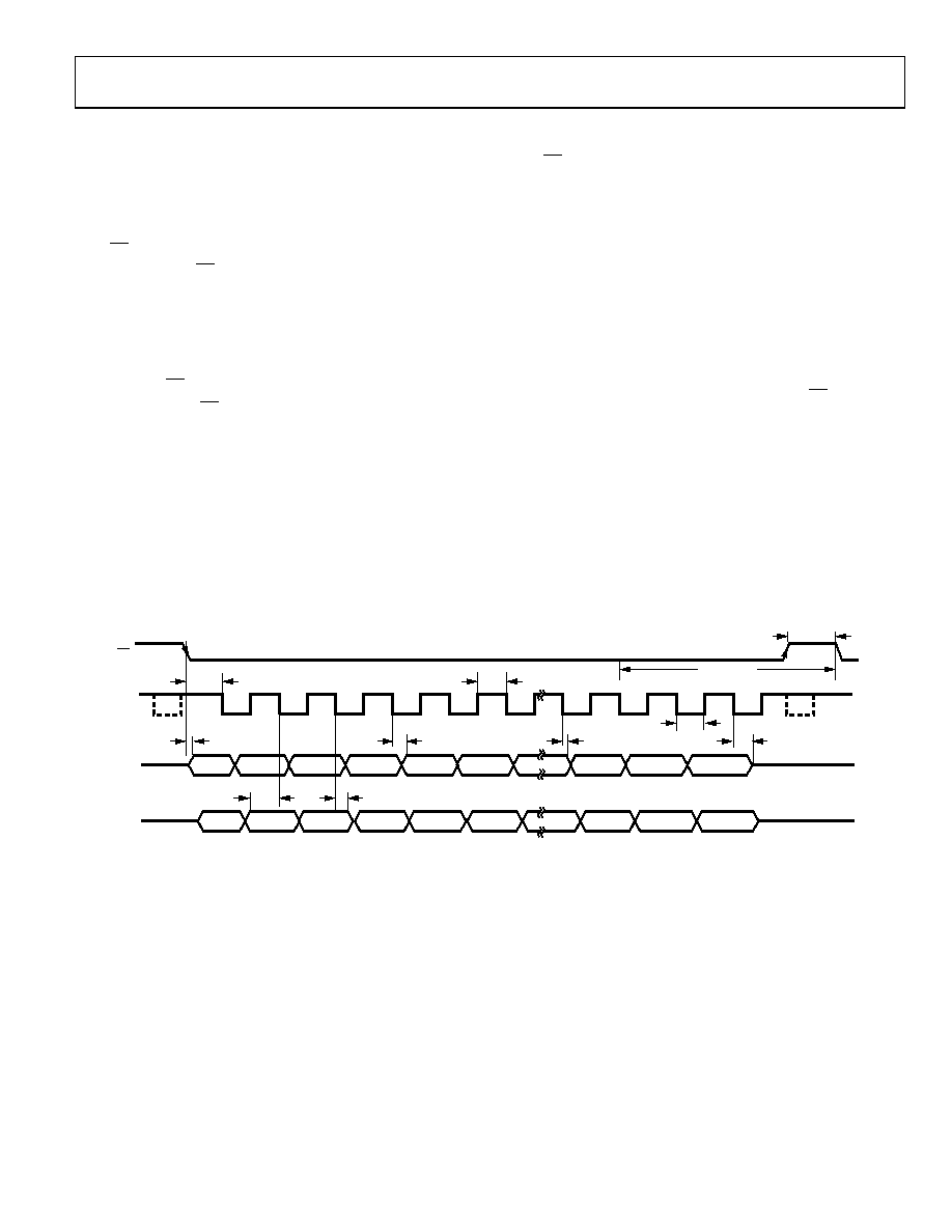
SERIAL INTERFACE
The CS going low provides the first address bit to be read in by
the microcontroller or DSP. The remaining data is then clocked
out by subsequent SCLK falling edges, beginning with a second
address bit. Thus, the first falling clock edge on the serial clock
has the first address bit provided for reading and also clocks out
the second address bit. The three remaining address bits and
12 data bits are clocked out by subsequent SCLK falling edges.
The final bit in the data transfer is valid for reading on the
16th falling edge having been clocked out on the previous (15th)
falling edge.
Figure 30 shows the detailed timing diagram for the serial
interface to the AD7298. The serial clock provides the conver-
sion clock and controls the transfer of information to and from
the AD7298 during each conversion.
The CS signal initiates the data transfer and conversion process.
The falling edge of CS puts the track-and-hold into hold mode
at which point the analog input is sampled and the bus is taken
out of three-state. The conversion is also initiated at this point
and requires 16 SCLK cycles to complete. The track-and-hold
goes back into track on the 14th SCLK falling edge as shown in
at Point B. On the 16th SCLK falling edge or on the
rising edge of
CS , the DOUT line goes back into three-state.
In applications with a slower SCLK, it may be possible to read
in data on each SCLK rising edge depending on the SCLK
frequency. The first rising edge of SCLK after the CS falling
edge would have the first address bit provided, and the 15th
rising SCLK edge would have last data bit provided.
If the rising edge of CS occurs before 16 SCLKs have elapsed,
the conversion is terminated, the DOUT line goes back into tri-
state, and the control register is not updated; otherwise, DOUT
returns to three-state on the 16th SCLK falling edge. Sixteen serial
clock cycles are required to perform the conversion process and
to access data from the AD7298.
Writing information to the control register takes place on the
first 16 falling edges of SCLK in a data transfer, assuming the MSB
(that is, the WRITE bit) has been set to 1. The 16-bit word read
from the AD7298 always contains four channel address bits that
the conversion result corresponds to, followed by the 12-bit
conversion result.
For the AD7298, four-channel address bits (ADD3 to ADD0)
that identify which channel the conversion result corresponds
to precede the 12 bits of data (see Table 9).
CS
DOUT
DIN
t2
t3
t9
t10
t4
t7
tACQUISITION
t8
tQUIET
t5
t6
SCLK
THREE-
STATE
THREE-
STATE
ADD3
WRITE
REPEAT
CH0
CH1
CH2
CH3
EXT_REF
PPD
TSENSEAVG
ADD2
12345
13
14
B
15
16
ADD1
ADD0
DB11
DB10
DB2
DB1
DB0
08
75
4-
01
4
Figure 30. Serial Interface Timing Diagram
相关PDF资料 |
PDF描述 |
|---|---|
| VI-24W-MY-B1 | CONVERTER MOD DC/DC 5.5V 50W |
| VE-JWD-MY-F3 | CONVERTER MOD DC/DC 85V 50W |
| VI-23Z-MY-B1 | CONVERTER MOD DC/DC 2V 20W |
| AD7887WARMZ | IC ADC 12BIT 2CH SRL 8-MSOP |
| VI-23Y-MX-B1 | CONVERTER MOD DC/DC 3.3V 49.5W |
相关代理商/技术参数 |
参数描述 |
|---|---|
| AD7298BCPZ-RL7 | 功能描述:IC ADC 10BIT SPI/SRL 8CH 20LFCSP RoHS:是 类别:集成电路 (IC) >> 数据采集 - 模数转换器 系列:- 标准包装:1,000 系列:- 位数:16 采样率(每秒):45k 数据接口:串行 转换器数目:2 功率耗散(最大):315mW 电压电源:模拟和数字 工作温度:0°C ~ 70°C 安装类型:表面贴装 封装/外壳:28-SOIC(0.295",7.50mm 宽) 供应商设备封装:28-SOIC W 包装:带卷 (TR) 输入数目和类型:2 个单端,单极 |
| AD73 | 制造商:Distributed By MCM 功能描述:REFRIGERATR DOOR GASKET DIRECT |
| AD7302 | 制造商:AD 制造商全称:Analog Devices 功能描述:2.7 V to 5.5 V, Parallel Input Dual Voltage Output 8-Bit DAC |
| AD7302BN | 功能描述:IC DAC 8BIT DUAL R-R 20-DIP RoHS:否 类别:集成电路 (IC) >> 数据采集 - 数模转换器 系列:- 标准包装:2,400 系列:- 设置时间:- 位数:18 数据接口:串行 转换器数目:3 电压电源:模拟和数字 功率耗散(最大):- 工作温度:-40°C ~ 85°C 安装类型:表面贴装 封装/外壳:36-TFBGA 供应商设备封装:36-TFBGA 包装:带卷 (TR) 输出数目和类型:* 采样率(每秒):* |
| AD7302BNZ | 功能描述:IC DAC 8BIT DUAL R-R 20-DIP RoHS:是 类别:集成电路 (IC) >> 数据采集 - 数模转换器 系列:- 产品培训模块:Lead (SnPb) Finish for COTS Obsolescence Mitigation Program 标准包装:50 系列:- 设置时间:4µs 位数:12 数据接口:串行 转换器数目:2 电压电源:单电源 功率耗散(最大):- 工作温度:-40°C ~ 85°C 安装类型:表面贴装 封装/外壳:8-TSSOP,8-MSOP(0.118",3.00mm 宽) 供应商设备封装:8-uMAX 包装:管件 输出数目和类型:2 电压,单极 采样率(每秒):* 产品目录页面:1398 (CN2011-ZH PDF) |
发布紧急采购,3分钟左右您将得到回复。