- 您现在的位置:买卖IC网 > PDF目录10681 > AD7298BCPZ (Analog Devices Inc)IC ADC 12BIT SPI/SRL 1M 20LFCSP PDF资料下载
参数资料
| 型号: | AD7298BCPZ |
| 厂商: | Analog Devices Inc |
| 文件页数: | 9/25页 |
| 文件大小: | 0K |
| 描述: | IC ADC 12BIT SPI/SRL 1M 20LFCSP |
| 特色产品: | AD7298 ADC with Temperature Sensor |
| 标准包装: | 1 |
| 位数: | 12 |
| 采样率(每秒): | 1M |
| 数据接口: | DSP,串行,SPI? |
| 转换器数目: | 1 |
| 功率耗散(最大): | 22.7mW |
| 电压电源: | 单电源 |
| 工作温度: | -40°C ~ 125°C |
| 安装类型: | 表面贴装 |
| 封装/外壳: | 20-WFQFN 裸露焊盘,CSP |
| 供应商设备封装: | 20-LFCSP-WQ(4x4) |
| 包装: | 托盘 |
| 输入数目和类型: | 8 个单端,单极 |
AD7298
Rev. B | Page 16 of 24
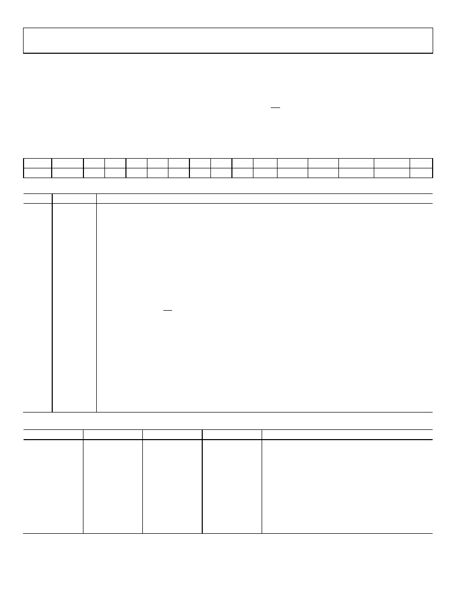
CONTROL REGISTER
The control register of the AD7298 is a 16-bit, write-only register. Data is loaded from the DIN pin of the AD7298 on the falling edge of
SCLK. The data is transferred on the DIN line at the same time that the conversion result is read from the part. The data transferred on
the DIN line corresponds to the AD7298 configuration for the next conversion. This requires 16 serial clocks for every data transfer. Only
the information provided on the first 16 falling clock edges (after the falling edge of CS) is loaded to the control register. MSB denotes the
first bit in the data stream. The bit functions are outlined in
and
. On power-up, the default content of the control register
is all zeros.
Table 7. Control Register Bit Functions
MSB
LSB
D15
D14
D13
D12
D11
D10
D9
D8
D7
D6
D5
D4
D3
D2
D1
D0
WRITE
REPEAT
CH0
CH1
CH2
CH3
CH4
CH5
CH6
CH7
TSENSE
DONTC
EXT_REF
TSENSEAVG
PPD
Table 8. Control Register Bit Function Description
Bit
Mnemonic
Description
D15
WRITE
The value written to this bit determines whether the subsequent 15 bits are loaded to the control register. If this
bit is a 1, the following 15 bits are written to the control register; if it is a 0, then the remaining 15 bits are not
loaded to the control register and it remains unchanged.
D14
REPEAT
This bit enables the repeated conversion of the selected sequence of channels.
D13 to
D6
CH0 to CH7
These eight channel selection bits are loaded at the end of the current conversion and select which analog input
channel is to be converted in the next serial transfer, or they may select the sequence of channels for conversion in
the subsequent serial transfers. Each CHX bit corresponds to an analog input channel. A channel or sequence of
channels is selected for conversion by writing a 1 to the appropriate CHX bit/bits. Channel address bits
corresponding to the conversion result are output on DOUT prior to the 12 bits of data. The next channel to be
converted is selected by the mux on the 14th SCLK falling edge.
D4
TSENSE
Writing a 1 to this bit enables the temperature conversion. When the temperature sensor is selected for
conversion, the TSENSE_BUSY pin goes high after the next CS falling edge to indicate that the conversion is in
progress; the previous conversion result can be read while the temperature conversion is in progress. Once
TSENSE_BUSY goes low, CS can be brought low 100 ns later to read the TSENSE conversion result.
4 to 3
DONTC
Don’t care.
D2
EXT_REF
Writing a Logic 1 to this bit, enables the use of an external reference. The input voltage range for the external
reference is 1 V to 2.5 V. The external reference should not exceed 2.5 V or the device performance is affected.
D1
TSENSEAVG
Writing a 1 to this bit enables the temperature sensor averaging function. When averaging is enabled, the AD7298
internally computes a running average of the conversion results to determine the final TSENSE result (see the
Temperature Sensor Averaging section for more details). This mode reduces the influence of noise on the final
TSENSE result. Selecting this feature does not automatically select the TSENSE for conversion. The TSENSE bit must also be
set to start a temperature sensor conversion.
D0
PPD
This partial power-down mode is selected by writing a 1 to this bit in the control register. In this mode, some of
the internal analog circuitry is powered down. The AD7298 retains the information in the control register while in
partial power-down mode. The part remains in this mode until a 0 is written to this bit.
Table 9. Channel Address Bits
ADD3
ADD2
ADD1
ADD0
Analog Input Channel
0
VIN0
0
1
VIN1
0
1
0
VIN2
0
1
VIN3
0
1
0
VIN4
0
1
0
1
VIN5
0
1
0
VIN6
0
1
VIN7
1
0
TSENSE
1
0
1
TSENSE with averaging enabled
相关PDF资料 |
PDF描述 |
|---|---|
| VI-24W-MY-B1 | CONVERTER MOD DC/DC 5.5V 50W |
| VE-JWD-MY-F3 | CONVERTER MOD DC/DC 85V 50W |
| VI-23Z-MY-B1 | CONVERTER MOD DC/DC 2V 20W |
| AD7887WARMZ | IC ADC 12BIT 2CH SRL 8-MSOP |
| VI-23Y-MX-B1 | CONVERTER MOD DC/DC 3.3V 49.5W |
相关代理商/技术参数 |
参数描述 |
|---|---|
| AD7298BCPZ-RL7 | 功能描述:IC ADC 10BIT SPI/SRL 8CH 20LFCSP RoHS:是 类别:集成电路 (IC) >> 数据采集 - 模数转换器 系列:- 标准包装:1,000 系列:- 位数:16 采样率(每秒):45k 数据接口:串行 转换器数目:2 功率耗散(最大):315mW 电压电源:模拟和数字 工作温度:0°C ~ 70°C 安装类型:表面贴装 封装/外壳:28-SOIC(0.295",7.50mm 宽) 供应商设备封装:28-SOIC W 包装:带卷 (TR) 输入数目和类型:2 个单端,单极 |
| AD73 | 制造商:Distributed By MCM 功能描述:REFRIGERATR DOOR GASKET DIRECT |
| AD7302 | 制造商:AD 制造商全称:Analog Devices 功能描述:2.7 V to 5.5 V, Parallel Input Dual Voltage Output 8-Bit DAC |
| AD7302BN | 功能描述:IC DAC 8BIT DUAL R-R 20-DIP RoHS:否 类别:集成电路 (IC) >> 数据采集 - 数模转换器 系列:- 标准包装:2,400 系列:- 设置时间:- 位数:18 数据接口:串行 转换器数目:3 电压电源:模拟和数字 功率耗散(最大):- 工作温度:-40°C ~ 85°C 安装类型:表面贴装 封装/外壳:36-TFBGA 供应商设备封装:36-TFBGA 包装:带卷 (TR) 输出数目和类型:* 采样率(每秒):* |
| AD7302BNZ | 功能描述:IC DAC 8BIT DUAL R-R 20-DIP RoHS:是 类别:集成电路 (IC) >> 数据采集 - 数模转换器 系列:- 产品培训模块:Lead (SnPb) Finish for COTS Obsolescence Mitigation Program 标准包装:50 系列:- 设置时间:4µs 位数:12 数据接口:串行 转换器数目:2 电压电源:单电源 功率耗散(最大):- 工作温度:-40°C ~ 85°C 安装类型:表面贴装 封装/外壳:8-TSSOP,8-MSOP(0.118",3.00mm 宽) 供应商设备封装:8-uMAX 包装:管件 输出数目和类型:2 电压,单极 采样率(每秒):* 产品目录页面:1398 (CN2011-ZH PDF) |
发布紧急采购,3分钟左右您将得到回复。