参数资料
| 型号: | AD7303BRM |
| 厂商: | Analog Devices Inc |
| 文件页数: | 15/16页 |
| 文件大小: | 0K |
| 描述: | IC DAC 8BIT DUAL R-R 8-MSOP |
| 产品培训模块: | Data Converter Fundamentals DAC Architectures |
| 标准包装: | 50 |
| 设置时间: | 1.2µs |
| 位数: | 8 |
| 数据接口: | 串行 |
| 转换器数目: | 2 |
| 电压电源: | 单电源 |
| 功率耗散(最大): | 6.93mW |
| 工作温度: | -40°C ~ 105°C |
| 安装类型: | 表面贴装 |
| 封装/外壳: | 8-TSSOP,8-MSOP(0.118",3.00mm 宽) |
| 供应商设备封装: | 8-MSOP |
| 包装: | 管件 |
| 输出数目和类型: | 2 电压,单极;2 电压,双极 |
| 采样率(每秒): | 833k |
AD7303
–8–
REV. 0
GENERAL DESCRIPTION
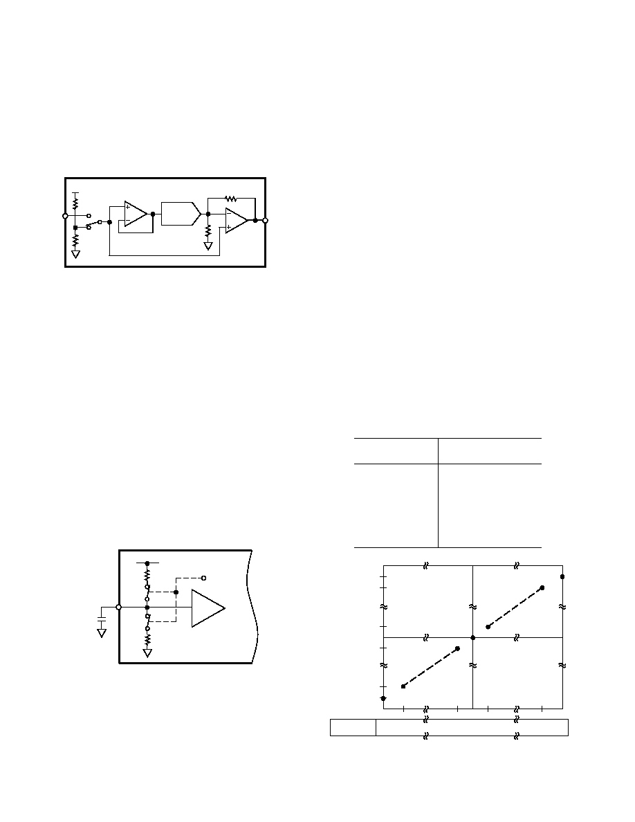
D/A Section
The AD7303 is a dual 8-bit voltage output digital-to-analog
converter. The architecture consists of a reference amplifier and
a current source DAC, followed by a current-to-voltage con-
verter capable of generating rail-to-rail voltages on the output of
the DAC. Figure 20 shows a block diagram of the basic DAC
architecture.
REFERENCE
AMPLIFIER
OUTPUT
AMPLIFIER
VO A/B
VDD
REF
AD7303
CURRENT
DAC
11.7k
30k
11.7k
30k
Figure 20. DAC Architecture
Both DAC A and DAC B outputs are internally buffered and
these output buffer amplifiers have rail-to-rail output character-
istics. The output amplifier is capable of driving a load of 10 k
to both VDD and ground and 100 pF to ground. The reference
selection for the DAC can be either internally generated from
VDD or externally applied through the REF pin. Reference
selection is via a bit in the control register. The range on the
external reference input is from 1.0 V to VDD/2. The output
voltage from either DAC is given by:
VO A/B = 2
× V
REF
× (N/256)
where:
VREF is the voltage applied to the external REF pin or
VDD/2 when the internal reference is selected.
N
is the decimal equivalent of the code loaded to the DAC
register and ranges from 0 to 255.
Reference
The AD7303 has the facility to use either an external reference
applied through the REF pin or an internal reference generated
from VDD. Figure 21 shows the reference input arrangement
where the internal VDD/2 has been selected.
30k
30k
REFERENCE
AMPLIFIER
AD7303
REF
0.1F
VDD
INT/EXT
Figure 21. Reference Input
When the internal reference is selected during the write to the
DAC, both switches are closed and VDD/2 is generated and
applied to the reference amplifier. This internal VDD/2 reference
appears at the reference pin as an output voltage for decoupling
purposes. When using the internal reference, external references
should not be connected to the REF Pin. This internal VDD/2
reference appears at the reference pin as an output voltage for
decoupling purposes. When using the internal reference, external
references should not be connected to the REF pin. If external ref-
erence is selected, both switches are open and the externally
applied voltage to the REF pin is applied to the reference amplifier.
Decoupling capacitors applied to the REF pin decouple both
the internal reference and external reference. In noisy environ-
ments it is recommended that a 0.1
F capacitor be connected
to the REF pin to provide added decoupling even when the in-
ternal reference is selected.
Analog Outputs
The AD7303 contains two independent voltage output DACs
with 8-bit resolution and rail-to-rail operation. The output buffer
provides a gain of two at the output. Figures 3 to 5 show the sink
and source capabilities of the output amplifier. The slew rate of the
output amplifier is typically 8 V/
s and has a full-scale settling to 8
bits with a 100 pF capacitive load in typically 1.2
s.
The input coding to the DAC is straight binary. Table I shows
the binary transfer function for the AD7303. Figure 22 shows
the DAC transfer function for binary coding. Any DAC output
voltage can ideally be expressed as:
VOUT = 2 × VREF (N/256)
where:
N
is the decimal equivalent of the binary input code.
N ranges from 0 to 255.
VREF is the voltage applied to the external REF pin when
the external reference is selected and is VDD/2 if the
internal reference is used.
Table I. Binary Code Table for AD7303 DAC
Digital Input
MSB . . . LSB
Analog Output
1111 1111
2
× 255/256 × V
REF V
1111 1110
2
× 254/256 × V
REF V
1000 0001
2
× 129/256 × V
REF V
1000 0000
VREF V
0111 1111
2
× 127/256 × V
REF V
0000 0001
2
× V
REF/256 V
0000 0000
0 V
2.VREF
VREF
0
DAC
OUTPUT
VOLTAGE
00
01
DAC INPUT
CODE
FF
80
81
FE
7F
Figure 22. DAC Transfer Function
相关PDF资料 |
PDF描述 |
|---|---|
| AD7305BRU | IC DAC 8BIT QUAD R-R 20-TSSOP |
| AD7321BRUZ-REEL7 | IC ADC 12BIT+ SAR 2CHAN 14TSSOP |
| AD7322BRUZ-REEL7 | IC ADC 12BIT+ SAR 2CHAN 14TSSOP |
| AD7323BRUZ-REEL7 | IC ADC 12BIT+ SAR 4CHAN 16TSSOP |
| AD7324BRUZ-REEL | IC ADC 12BIT+SAR 4CHAN 16-TSSOP |
相关代理商/技术参数 |
参数描述 |
|---|---|
| AD7303BRM-REEL | 制造商:Analog Devices 功能描述:DAC 2-CH Current Steering 8-bit 8-Pin MSOP T/R 制造商:Analog Devices 功能描述:DAC 2CH CURRENT STEERING 8BIT 8MSOP - Tape and Reel 制造商:Rochester Electronics LLC 功能描述:DUAL SERIAL 8-BIT SINGLE SUPPLY DAC I.C. - Tape and Reel |
| AD7303BRM-REEL7 | 功能描述:IC DAC 8BIT DUAL R-R 8-MSOP T/R RoHS:否 类别:集成电路 (IC) >> 数据采集 - 数模转换器 系列:- 标准包装:2,400 系列:- 设置时间:- 位数:18 数据接口:串行 转换器数目:3 电压电源:模拟和数字 功率耗散(最大):- 工作温度:-40°C ~ 85°C 安装类型:表面贴装 封装/外壳:36-TFBGA 供应商设备封装:36-TFBGA 包装:带卷 (TR) 输出数目和类型:* 采样率(每秒):* |
| AD7303BRMZ | 功能描述:IC DAC 8BIT DUAL R-R 8-MSOP RoHS:是 类别:集成电路 (IC) >> 数据采集 - 数模转换器 系列:- 产品培训模块:Lead (SnPb) Finish for COTS Obsolescence Mitigation Program 标准包装:50 系列:- 设置时间:4µs 位数:12 数据接口:串行 转换器数目:2 电压电源:单电源 功率耗散(最大):- 工作温度:-40°C ~ 85°C 安装类型:表面贴装 封装/外壳:8-TSSOP,8-MSOP(0.118",3.00mm 宽) 供应商设备封装:8-uMAX 包装:管件 输出数目和类型:2 电压,单极 采样率(每秒):* 产品目录页面:1398 (CN2011-ZH PDF) |
| AD7303BRMZ-REEL | 功能描述:IC DAC 8BIT DUAL R-R 8-MSOP RoHS:是 类别:集成电路 (IC) >> 数据采集 - 数模转换器 系列:- 产品培训模块:LTC263x 12-, 10-, and 8-Bit VOUT DAC Family 特色产品:LTC2636 - Octal 12-/10-/8-Bit SPI VOUT DACs with 10ppm/°C Reference 标准包装:91 系列:- 设置时间:4µs 位数:10 数据接口:MICROWIRE?,串行,SPI? 转换器数目:8 电压电源:单电源 功率耗散(最大):2.7mW 工作温度:-40°C ~ 85°C 安装类型:表面贴装 封装/外壳:14-WFDFN 裸露焊盘 供应商设备封装:14-DFN-EP(4x3) 包装:管件 输出数目和类型:8 电压,单极 采样率(每秒):* |
| AD7303BRMZ-REEL7 | 功能描述:IC DAC 8BIT DUAL R-R 8-MSOP RoHS:是 类别:集成电路 (IC) >> 数据采集 - 数模转换器 系列:- 产品培训模块:LTC263x 12-, 10-, and 8-Bit VOUT DAC Family 特色产品:LTC2636 - Octal 12-/10-/8-Bit SPI VOUT DACs with 10ppm/°C Reference 标准包装:91 系列:- 设置时间:4µs 位数:10 数据接口:MICROWIRE?,串行,SPI? 转换器数目:8 电压电源:单电源 功率耗散(最大):2.7mW 工作温度:-40°C ~ 85°C 安装类型:表面贴装 封装/外壳:14-WFDFN 裸露焊盘 供应商设备封装:14-DFN-EP(4x3) 包装:管件 输出数目和类型:8 电压,单极 采样率(每秒):* |
发布紧急采购,3分钟左右您将得到回复。