- 您现在的位置:买卖IC网 > PDF目录10745 > AD73360LARZ-REEL7 (Analog Devices Inc)IC PROCESSOR FRONTEND 6CH 28SOIC PDF资料下载
参数资料
| 型号: | AD73360LARZ-REEL7 |
| 厂商: | Analog Devices Inc |
| 文件页数: | 5/35页 |
| 文件大小: | 0K |
| 描述: | IC PROCESSOR FRONTEND 6CH 28SOIC |
| 标准包装: | 400 |
| 位数: | 16 |
| 通道数: | 6 |
| 功率(瓦特): | 80mW |
| 电压 - 电源,模拟: | 3V |
| 电压 - 电源,数字: | 3V |
| 封装/外壳: | 28-SOIC(0.295",7.50mm 宽) |
| 供应商设备封装: | 28-SOIC W |
| 包装: | 带卷 (TR) |
第1页第2页第3页第4页当前第5页第6页第7页第8页第9页第10页第11页第12页第13页第14页第15页第16页第17页第18页第19页第20页第21页第22页第23页第24页第25页第26页第27页第28页第29页第30页第31页第32页第33页第34页第35页
REV. A
AD73360
–13–
Serial Port (SPORT)
The AD73360s communicate with a host processor via the
bidirectional synchronous serial port (SPORT) which is compat-
ible with most modern DSPs. The SPORT is used to transmit
and receive digital data and control information. Multiple
AD73360s be cascaded together (up to a limit of eight) to pro-
vide additional input channels.
In both transmit and receive modes, data is transferred at the
serial clock (SCLK) rate with the MSB being transferred first.
Due to the fact that the SPORT of each AD73360 block uses a
common serial register for serial input and output, communica-
tions between an AD73360 and a host processor (DSP engine)
must always be initiated by the AD73360s themselves. In this
configuration the AD73360s are described as being in Master
mode. This ensures that there is no collision between input data
and output samples.
SPORT Overview
The AD73360 SPORT is a flexible, full-duplex, synchronous
serial port whose protocol has been designed to allow up to
eight AD73360 devices to be connected in cascade, to a single
DSP via a six-wire interface. It has a very flexible architecture
that can be configured by programming two of the internal
control registers in each device. The AD73360 SPORT has
three distinct modes of operation: Control Mode, Data Mode
and Mixed Control/Data Mode.
NOTE: As each AD73360 has its own SPORT section, the
register settings in both SPORTs must be programmed. The
registers which control SPORT and sample rate operation (CRA
and CRB) must be programmed with the same values, otherwise
incorrect operation may occur.
In Program Mode (CRA:0 = 0), the device’s internal configura-
tion can be programmed by writing to the eight internal control
registers. In this mode, control information can be written to or
read from the AD73360. In Data Mode (CRA:0 = 1), any infor-
mation that is sent to the device is ignored, while the encoder
section (ADC) data is read from the device. In this mode, only
ADC data is read from the device. Mixed mode (CRA:0 = 1
and CRA:1 = 1) allows the user to send control information and
receive either control information or ADC data. This is achieved
by using the MSB of the 16-bit frame as a flag bit. Mixed mode
reduces the resolution to 15 bits with the MSB being used to
indicate whether the information in the 16-bit frame is control
information or ADC data.
The SPORT features a single 16-bit serial register that is used
for both input and output data transfers. As the input and out-
put data must share the same register there are some precau-
tions that must be observed. The primary precaution is that no
information must be written to the SPORT without reference to
an output sample event, which is when the serial register will be
overwritten with the latest ADC sample word. Once the SPORT
starts to output the latest ADC word, it is safe for the DSP to
write new control words to the AD73360. In certain configura-
tions, data can be written to the device to coincide with the
output sample being shifted out of the serial register—see section
on interfacing devices. The serial clock rate (CRB:2–3) defines
how many 16-bit words can be written to a device before the
next output sample event will happen.
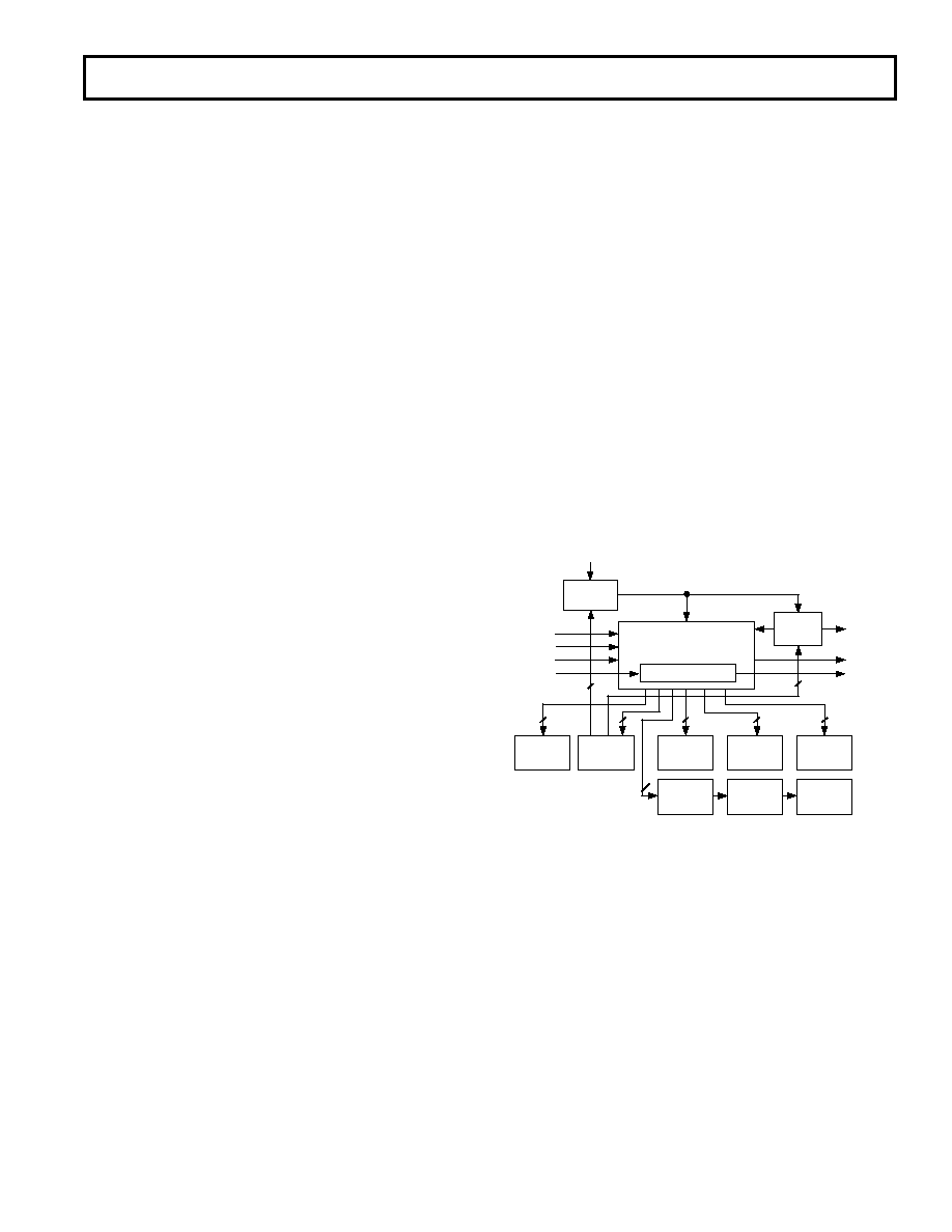
The SPORT block diagram, shown in Figure 9, details the blocks
associated with AD73360 including the eight control registers
(A–H), external MCLK to internal DMCLK divider and serial
clock divider. The divider rates are controlled by the setting of
Control Register B. The AD73360 features a master clock
divider that allows users the flexibility of dividing externally
available high frequency DSP or CPU clocks to generate a lower
frequency master clock internally in the AD73360 which may be
more suitable for either serial transfer or sampling rate require-
ments. The master clock divider has five divider options (
÷1
default condition,
÷2, ÷3, ÷4, ÷5) that are set by loading the
master clock divider field in Register B with the appropriate
code (see Table VI). Once the internal device master clock
(DMCLK) has been set using the master clock divider, the
sample rate and serial clock settings are derived from DMCLK.
MCLK
DIVIDER
MCLK
(EXTERNAL)
SE
RESET
SDIFS
SDI
SERIAL PORT
(SPORT)
SERIAL REGISTER
SCLK
CONTROL
REGISTER
B
CONTROL
REGISTER
C
CONTROL
REGISTER
D
CONTROL
REGISTER
E
CONTROL
REGISTER
A
3
8
2
DMCLK
(INTERNAL)
SDOFS
SDO
CONTROL
REGISTER
F
CONTROL
REGISTER
G
CONTROL
REGISTER
H
SCLK
DIVIDER
Figure 9. SPORT Block Diagram
The SPORT can work at four different serial clock (SCLK)
rates: chosen from DMCLK, DMCLK/2, DMCLK/4 or
DMCLK/8, where DMCLK is the internal or device master
clock resulting from the external or pin master clock being di-
vided by the master clock divider. Care should be taken when
selecting Master Clock, Serial Clock and Sample Rate divider
settings to ensure that there is sufficient time to read all the data
from the AD73360 before the next sample interval.
相关PDF资料 |
PDF描述 |
|---|---|
| MAX965EUA+ | IC COMPARATOR R-R 8-UMAX |
| MAX966ESA+ | IC COMPARATOR R-R 8-SOIC |
| VE-JN4-MY-F1 | CONVERTER MOD DC/DC 48V 50W |
| MAX965ESA+ | IC COMPARATOR R-R 8-SOIC |
| VE-JN3-MY-F4 | CONVERTER MOD DC/DC 24V 50W |
相关代理商/技术参数 |
参数描述 |
|---|---|
| AD7339 | 制造商:AD 制造商全称:Analog Devices 功能描述:5 V Integrated High Speed ADC/Quad DAC System |
| AD7339BS | 制造商:Analog Devices 功能描述:Data Acquisition System Single ADC Quad DAC 8-Bit 52-Pin MQFP |
| AD7339BS-REEL | 制造商:Analog Devices 功能描述:Data Acquisition System Single ADC Quad DAC 8-Bit 52-Pin MQFP T/R |
| AD7339BSZ-REEL | 功能描述:IC ADC/QUAD DAC 5V W/REF 52-MQFP RoHS:是 类别:集成电路 (IC) >> 数据采集 - ADCs/DAC - 专用型 系列:- 产品培训模块:Lead (SnPb) Finish for COTS Obsolescence Mitigation Program 标准包装:50 系列:- 类型:数据采集系统(DAS) 分辨率(位):16 b 采样率(每秒):21.94k 数据接口:MICROWIRE?,QSPI?,串行,SPI? 电压电源:模拟和数字 电源电压:1.8 V ~ 3.6 V 工作温度:-40°C ~ 85°C 安装类型:表面贴装 封装/外壳:40-WFQFN 裸露焊盘 供应商设备封装:40-TQFN-EP(6x6) 包装:托盘 |
| AD734 | 制造商:AD 制造商全称:Analog Devices 功能描述:10 MHz, 4-Quadrant Multiplier/Divider |
发布紧急采购,3分钟左右您将得到回复。