- 您现在的位置:买卖IC网 > PDF目录10289 > AD7352BRUZ-RL (Analog Devices Inc)IC ADC DUAL 12BIT 3MSPS 16TSSOP PDF资料下载
参数资料
| 型号: | AD7352BRUZ-RL |
| 厂商: | Analog Devices Inc |
| 文件页数: | 6/21页 |
| 文件大小: | 0K |
| 描述: | IC ADC DUAL 12BIT 3MSPS 16TSSOP |
| 设计资源: | DC-Coupled, Single-Ended-to-Differential Conversion Using AD8138 and AD7352 (CN0040) |
| 标准包装: | 2,500 |
| 位数: | 12 |
| 采样率(每秒): | 3M |
| 数据接口: | DSP,MICROWIRE?,QSPI?,串行,SPI? |
| 转换器数目: | 2 |
| 功率耗散(最大): | 45mW |
| 电压电源: | 单电源 |
| 工作温度: | -40°C ~ 85°C |
| 安装类型: | 表面贴装 |
| 封装/外壳: | 16-TSSOP(0.173",4.40mm 宽) |
| 供应商设备封装: | 16-TSSOP |
| 包装: | 带卷 (TR) |
| 输入数目和类型: | 2 个差分,双极 |
AD7352
Rev. A | Page 13 of 20
For ac applications, removing high frequency components from
the analog input signal is recommended by the use of an RC
low-pass filter on the analog input pins. In applications where
harmonic distortion and signal-to-noise ratio are critical, the
analog input should be driven from a low impedance source.
Large source impedances significantly affect the ac perfor-
mance of the ADC and may necessitate the use of an input
buffer amplifier. The choice of the op amp is a function of the
particular application.
When no amplifier is used to drive the analog input, limit
the source impedance to low values. The maximum source
impedance depends on the amount of THD that can be
tolerated. THD increases as the source impedance increases
and performance degrades. Figure 17 shows a graph of THD
vs. the analog input signal frequency for different source
impedances.
–89
–87
–85
–83
–81
–79
–77
–75
–73
–71
–69
–67
–65
100
500
1000
1500
2000
2500
T
HD
(
d
B)
FREQUENCY (kHz)
070
44
-027
100
50
33
10
Figure 17. THD vs. Analog Input Signal Frequency for Various Source
Impedances
Figure 18 shows a graph of the THD vs. the analog input
frequency while sampling at 3 MSPS. In this case, the source
impedance is 33 Ω.
–90
–86
–82
–78
–74
–70
–66
0
1000 2000 3000 4000 5000 6000 7000 8000 9000 10000
T
HD
(
d
B)
ANALOG INPUT FREQUENCY (kHz)
070
44
-028
Figure 18. THD vs. Analog Input Frequency
ANALOG INPUTS
Differential signals have some benefits over single-ended
signals, including noise immunity based on the devices
common-mode rejection and improvements in distortion
performance. Figure 19 defines the fully differential input of
the AD7352.
VIN+
AD7352*
VIN–
VREF p-p
*ADDITIONAL PINS OMITTED FOR CLARITY.
COMMON-MODE
VOLTAGE
07
04
4-
0
39
Figure 19. Differential Input Definition
The amplitude of the differential signal is the difference
between the signals applied to the VIN+ and VIN pins in
each differential pair (VIN+ VIN). VIN+ and VIN should be
simultaneously driven by two signals each of amplitude (VREF)
that are 180° out of phase. This amplitude of the differential
signal is, therefore VREF to +VREF peak-to-peak regardless of
the common mode (CM).
CM is the average of the two signals and is, therefore, the
voltage on which the two inputs are centered.
CM = (VIN+ + VIN)/2
This results in the span of each input being CM ± VREF/2. This
voltage has to be set up externally. When setting up the CM,
ensure that VIN+ and VIN remain within GND/VDD. When
a conversion takes place, CM is rejected, resulting in a virtually
noise-free signal of amplitude, VREF to +VREF, corresponding
to the digital codes of 0 to 4095 for the AD7352.
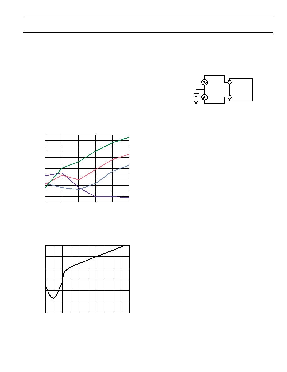
DRIVING DIFFERENTIAL INPUTS
Differential operation requires VIN+ and VIN to be driven
simultaneously with two equal signals that are 180° out of
phase. Because not all applications have a signal preconditioned
for differential operation, there is often a need to perform a
single-ended-to-differential conversion.
Differential Amplifier
An ideal method of applying differential drive to the AD7352
is to use a differential amplifier such as the AD8138. This part
can be used as a single-ended-to-differential amplifier or as a
differential-to-differential amplifier. The AD8138 also provides
can be used as a single-ended-to-differential amplifier. The
positive and negative outputs of the AD8138 are connected to
the respective inputs on the ADC via a pair of series resistors
to minimize the effects of switched capacitance on the front end
of the ADC. The architecture of the AD8138 results in outputs
that are very highly balanced over a wide frequency range
without requiring tightly matched external components.
相关PDF资料 |
PDF描述 |
|---|---|
| LTC1407HMSE#TRPBF | IC ADC 12BIT 3MSPS 10-MSOP |
| LTC1854CG#PBF | IC ADC 12BIT 8CH 100KSPS 28SSOP |
| D38999/26MC4AA | CONN HSG PLUG 4POS STRGHT PINS |
| MS27468T13F4P | CONN RCPT 4POS JAM NUT W/PINS |
| MS27467T25F24SLC | CONN HSG PLUG 24POS STRGHT SCKT |
相关代理商/技术参数 |
参数描述 |
|---|---|
| AD7352YRUZ | 功能描述:IC ADC DUAL 12BIT 3MSPS 16TSSOP RoHS:是 类别:集成电路 (IC) >> 数据采集 - 模数转换器 系列:- 其它有关文件:TSA1204 View All Specifications 标准包装:1 系列:- 位数:12 采样率(每秒):20M 数据接口:并联 转换器数目:2 功率耗散(最大):155mW 电压电源:模拟和数字 工作温度:-40°C ~ 85°C 安装类型:表面贴装 封装/外壳:48-TQFP 供应商设备封装:48-TQFP(7x7) 包装:Digi-Reel® 输入数目和类型:4 个单端,单极;2 个差分,单极 产品目录页面:1156 (CN2011-ZH PDF) 其它名称:497-5435-6 |
| AD7352YRUZ-500RL7 | 功能描述:IC ADC DUAL 12BIT 3MSPS 16TSSOP RoHS:是 类别:集成电路 (IC) >> 数据采集 - 模数转换器 系列:- 标准包装:1,000 系列:- 位数:16 采样率(每秒):45k 数据接口:串行 转换器数目:2 功率耗散(最大):315mW 电压电源:模拟和数字 工作温度:0°C ~ 70°C 安装类型:表面贴装 封装/外壳:28-SOIC(0.295",7.50mm 宽) 供应商设备封装:28-SOIC W 包装:带卷 (TR) 输入数目和类型:2 个单端,单极 |
| AD7352YRUZ-RL | 功能描述:IC ADC DUAL 12BIT 3MSPS 16TSSOP RoHS:是 类别:集成电路 (IC) >> 数据采集 - 模数转换器 系列:- 标准包装:1,000 系列:- 位数:16 采样率(每秒):45k 数据接口:串行 转换器数目:2 功率耗散(最大):315mW 电压电源:模拟和数字 工作温度:0°C ~ 70°C 安装类型:表面贴装 封装/外壳:28-SOIC(0.295",7.50mm 宽) 供应商设备封装:28-SOIC W 包装:带卷 (TR) 输入数目和类型:2 个单端,单极 |
| AD7356 | 制造商:AD 制造商全称:Analog Devices 功能描述:Differential Input,Dual,Simultaneous Sampling, 4.25 MSPS, 14-Bit, SAR ADC |
| AD7356_08 | 制造商:AD 制造商全称:Analog Devices 功能描述:Differential Input, Dual, Simultaneous Sampling, 5 MSPS, 12-Bit, SAR ADC |
发布紧急采购,3分钟左右您将得到回复。