- 您现在的位置:买卖IC网 > PDF目录10664 > AD7357BRUZ (Analog Devices Inc)IC ADC DUAL14BIT 4.2MSPS 16TSSOP PDF资料下载
参数资料
| 型号: | AD7357BRUZ |
| 厂商: | Analog Devices Inc |
| 文件页数: | 6/21页 |
| 文件大小: | 0K |
| 描述: | IC ADC DUAL14BIT 4.2MSPS 16TSSOP |
| 设计资源: | DC-Coupled, Single-Ended-to-Differential Conversion Using AD8138 and AD7357 (CN0061) |
| 标准包装: | 1 |
| 位数: | 14 |
| 采样率(每秒): | 4.2M |
| 数据接口: | DSP,MICROWIRE?,QSPI?,串行,SPI? |
| 转换器数目: | 2 |
| 功率耗散(最大): | 59mW |
| 电压电源: | 单电源 |
| 工作温度: | -40°C ~ 85°C |
| 安装类型: | 表面贴装 |
| 封装/外壳: | 16-TSSOP(0.173",4.40mm 宽) |
| 供应商设备封装: | 16-TSSOP |
| 包装: | 管件 |
| 输入数目和类型: | 2 个差分,双极 |
| 产品目录页面: | 777 (CN2011-ZH PDF) |
AD7357
Rev. B | Page 13 of 20
For ac applications, it is recommended to remove high frequency
components from the analog input signal by the use of an RC
low-pass filter on the analog input pins. In applications where
harmonic distortion and signal-to-noise ratio are critical, the
analog input should be driven from a low impedance source. Large
source impedances significantly affect the ac performance of the
ADC and may necessitate the use of an input buffer amplifier.
The choice of the op amp is a function of the particular
application.
When no amplifier is used to drive the analog input, the source
impedance should be limited to low values. The maximum source
impedance depends on the amount of THD that can be tole-
rated. The THD increases as the source impedance increases
and performance degrades. Figure 17 shows a graph of the
THD vs. the analog input signal frequency for various source
impedances.
–89
–87
–85
–83
–81
–79
–77
–75
–73
–71
–69
–67
–65
100
200
1000
1500
2000
2500
FREQUENCY (kHz)
T
HD
(
d
B)
10
33
50
100
07
75
7-
01
7
Figure 17. THD vs. Analog Input Frequency for Various Source Impedances
Figure 18 shows a graph of the THD vs. the analog input
frequency while sampling at 4.2 MSPS. In this case, the
source impedance is 33 Ω.
–90.0
–86.0
–82.0
–78.0
–74.0
–70.0
–66.0
0
1000
2000
3000
4000
5000
ANALOG INPUT FREQUENCY (kHz)
T
HD
(
d
B)
07
75
7–
11
8
Figure 18. THD vs. Analog Input Frequency
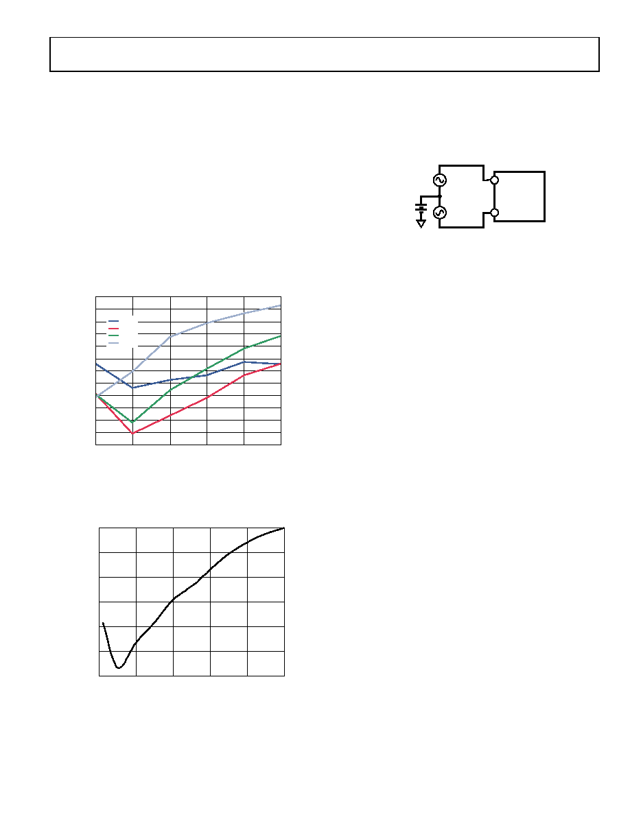
ANALOG INPUTS
Differential signals have some benefits over single-ended
signals, including noise immunity based on the device’s
common-mode rejection and improvements in distortion
performance. Figure 19 defines the fully differential input
of the AD7357.
VIN+
AD7357*
VIN–
VREF p-p
*ADDITIONAL PINS OMITTED FOR CLARITY.
COMMON
MODE
VOLTAGE
0
775
7-
03
4
Figure 19. Differential Input Definition
The amplitude of the differential signal is the difference
between the signals applied to the VIN+ and VIN pins in
each differential pair (VIN+ VIN). VIN+ and VIN should be
simultaneously driven by two signals each of amplitude VREF
that are 180° out of phase. This amplitude of the differential
signal is, therefore, –VREF to +VREF peak-to-peak regardless of
the common mode (CM).
CM is the average of the two signals and is, therefore, the
voltage on which the two inputs are centered.
CM = (VIN+ + VIN)/2
This results in the span of each input being CM ± VREF/2. This
voltage has to be set up externally. When setting up the CM,
ensure that that VIN+ and VIN remain within GND/VDD. When
a conversion takes place, CM is rejected, resulting in a virtually
noise free signal of amplitude –VREF to +VREF corresponding to
the digital codes of 0 to 16,383.
DRIVING DIFFERENTIAL INPUTS
Differential operation requires VIN+ and VIN to be driven simulta-
neously with two equal signals that are 180° out of phase. Because
not all applications have a signal preconditioned for differential
operation, there is often a need to perform a single-ended-to-
differential conversion.
Differential Amplifier
An ideal method of applying differential drive to the AD7357
is to use a differential amplifier such as the AD8138. This part
can be used as a single-ended-to-differential amplifier or as a
differential-to-differential amplifier. The AD8138 also provides
can be used as a single-ended-to-differential amplifier. The
positive and negative outputs of the AD8138 are connected to
the respective inputs on the ADC via a pair of series resistors
to minimize the effects of switched capacitance on the front
end of the ADC. The architecture of the AD8138 results in
outputs that are very highly balanced over a wide frequency
range without requiring tightly matched external components.
相关PDF资料 |
PDF描述 |
|---|---|
| AD7731BRZ | IC ADC 24BIT SIGMA-DELTA 24-SOIC |
| LTC2355IMSE-14#PBF | IC ADC 14BIT 3.5MSPS 10-MSOP |
| MAX9092AUA+T | IC COMPARATOR GP DUAL 8UMAX |
| VI-B13-MX-F4 | CONVERTER MOD DC/DC 24V 75W |
| LTC2356IMSE-14#PBF | IC ADC 14BIT 3.5MSPS 10-MSOP |
相关代理商/技术参数 |
参数描述 |
|---|---|
| AD7357BRUZ-500RL7 | 功能描述:IC ADC DUAL14BIT 4.2MSPS 16TSSOP RoHS:是 类别:集成电路 (IC) >> 数据采集 - 模数转换器 系列:- 标准包装:1,000 系列:- 位数:12 采样率(每秒):300k 数据接口:并联 转换器数目:1 功率耗散(最大):75mW 电压电源:单电源 工作温度:0°C ~ 70°C 安装类型:表面贴装 封装/外壳:24-SOIC(0.295",7.50mm 宽) 供应商设备封装:24-SOIC 包装:带卷 (TR) 输入数目和类型:1 个单端,单极;1 个单端,双极 |
| AD7357BRUZ-RL | 功能描述:IC ADC 14BITDUAL 4.MSPS 16TSSOP RoHS:是 类别:集成电路 (IC) >> 数据采集 - 模数转换器 系列:- 标准包装:1,000 系列:- 位数:12 采样率(每秒):300k 数据接口:并联 转换器数目:1 功率耗散(最大):75mW 电压电源:单电源 工作温度:0°C ~ 70°C 安装类型:表面贴装 封装/外壳:24-SOIC(0.295",7.50mm 宽) 供应商设备封装:24-SOIC 包装:带卷 (TR) 输入数目和类型:1 个单端,单极;1 个单端,双极 |
| AD7357WYRUZ | 制造商:Analog Devices 功能描述:ADC Dual SAR 4.2Msps 14-bit Serial 16-Pin TSSOP 制造商:Analog Devices 功能描述:14-BIT DUAL DIFF SIMULT 5 MSPS ADC I.C. - Rail/Tube 制造商:Rochester Electronics LLC 功能描述: 制造商:Analog Devices 功能描述:IC ADC 14BIT SRL 5MSPS 16TSSOP 制造商:Analog Devices 功能描述:Analog to Digital Converters - ADC 14-Bit Dual Diff Simult 5 MSPS 制造商:Analog Devices 功能描述:14-Bit Dual Diff Simult 5 MSPS ADC I.C. |
| AD7357WYRUZ-RL | 功能描述:模数转换器 - ADC 14-Bit Dual Diff Simult 5 MSPS RoHS:否 制造商:Analog Devices 通道数量: 结构: 转换速率: 分辨率: 输入类型: 信噪比: 接口类型: 工作电源电压: 最大工作温度: 安装风格: 封装 / 箱体: |
| AD7357YRUZ | 功能描述:IC ADC DUAL14BIT 4.2MSPS 16TSSOP RoHS:是 类别:集成电路 (IC) >> 数据采集 - 模数转换器 系列:- 标准包装:1 系列:- 位数:14 采样率(每秒):83k 数据接口:串行,并联 转换器数目:1 功率耗散(最大):95mW 电压电源:双 ± 工作温度:0°C ~ 70°C 安装类型:通孔 封装/外壳:28-DIP(0.600",15.24mm) 供应商设备封装:28-PDIP 包装:管件 输入数目和类型:1 个单端,双极 |
发布紧急采购,3分钟左右您将得到回复。