- 您现在的位置:买卖IC网 > PDF目录10322 > AD7440BRTZ-R2 (Analog Devices Inc)IC ADC 10BIT W/DIFF INP SOT-23-8 PDF资料下载
参数资料
| 型号: | AD7440BRTZ-R2 |
| 厂商: | Analog Devices Inc |
| 文件页数: | 13/29页 |
| 文件大小: | 0K |
| 描述: | IC ADC 10BIT W/DIFF INP SOT-23-8 |
| 标准包装: | 1 |
| 位数: | 10 |
| 采样率(每秒): | 1M |
| 数据接口: | DSP,MICROWIRE?,QSPI?,串行,SPI? |
| 转换器数目: | 1 |
| 功率耗散(最大): | 9.25mW |
| 电压电源: | 单电源 |
| 工作温度: | -40°C ~ 85°C |
| 安装类型: | 表面贴装 |
| 封装/外壳: | SOT-23-8 |
| 供应商设备封装: | SOT-23-8 |
| 包装: | 标准包装 |
| 输入数目和类型: | 1 个差分,单极 |
| 其它名称: | AD7440BRTZ-R2DKR |
第1页第2页第3页第4页第5页第6页第7页第8页第9页第10页第11页第12页当前第13页第14页第15页第16页第17页第18页第19页第20页第21页第22页第23页第24页第25页第26页第27页第28页第29页
AD7440/AD7450A
Rev. C | Page 19 of 28
Op Amp Pair
An op amp pair can be used to directly couple a differential
signal to the AD7440/AD7450A. The circuit configurations
be used to convert a single-ended signal into a differential
signal for both a bipolar and unipolar input signal, respectively.
The voltage applied to Point A sets up the common-mode
voltage. In both diagrams, it is connected in some way to the
reference, but any value in the common-mode range can be
input here to set up the common mode. The AD8022 is a
suitable dual op amp that could be used in this configuration
to provide differential drive to the AD7440/AD7450A.
Take care when choosing the op amp; the selection depends on
the required power supply and system performance objectives.
dc coupling applications requiring best distortion performance.
The circuit configuration shown in Figure 35 converts a
unipolar, single-ended signal into a differential signal.
The differential op amp driver circuit in Figure 36 is configured
to convert and level shift a single-ended, ground-referenced
(bipolar) signal to a differential signal centered at the VREF level
of the ADC.
03051-
A
-036
VDD
2
× V
REF p-p
VREF
GND
390
Ω
220
Ω
220
Ω
220
Ω
10k
Ω
27
Ω
27
Ω
0.1
μF
V+
V–
V+
V–
A
VIN+
VIN–
VREF
AD7440/
AD7450A
EXTERNAL
VREF
Figure 35. Dual Op Amp Circuit to Convert a Single-Ended Unipolar Signal
into a Differential Signal
03051-A-035
GND
V+
V–
V+
V–
A
VIN+
VDD
VIN–
VREF
AD7440/
AD7450A
2
× V
REF p-p
390
Ω
220
Ω
220
Ω
220
Ω
220
Ω
10k
Ω
20k
Ω
27
Ω
27
Ω
0.1
μF
EXTERNAL
VREF
Figure 36. Dual Op Amp Circuit to Convert a Single-Ended Bipolar Signal into
a Differential Signal
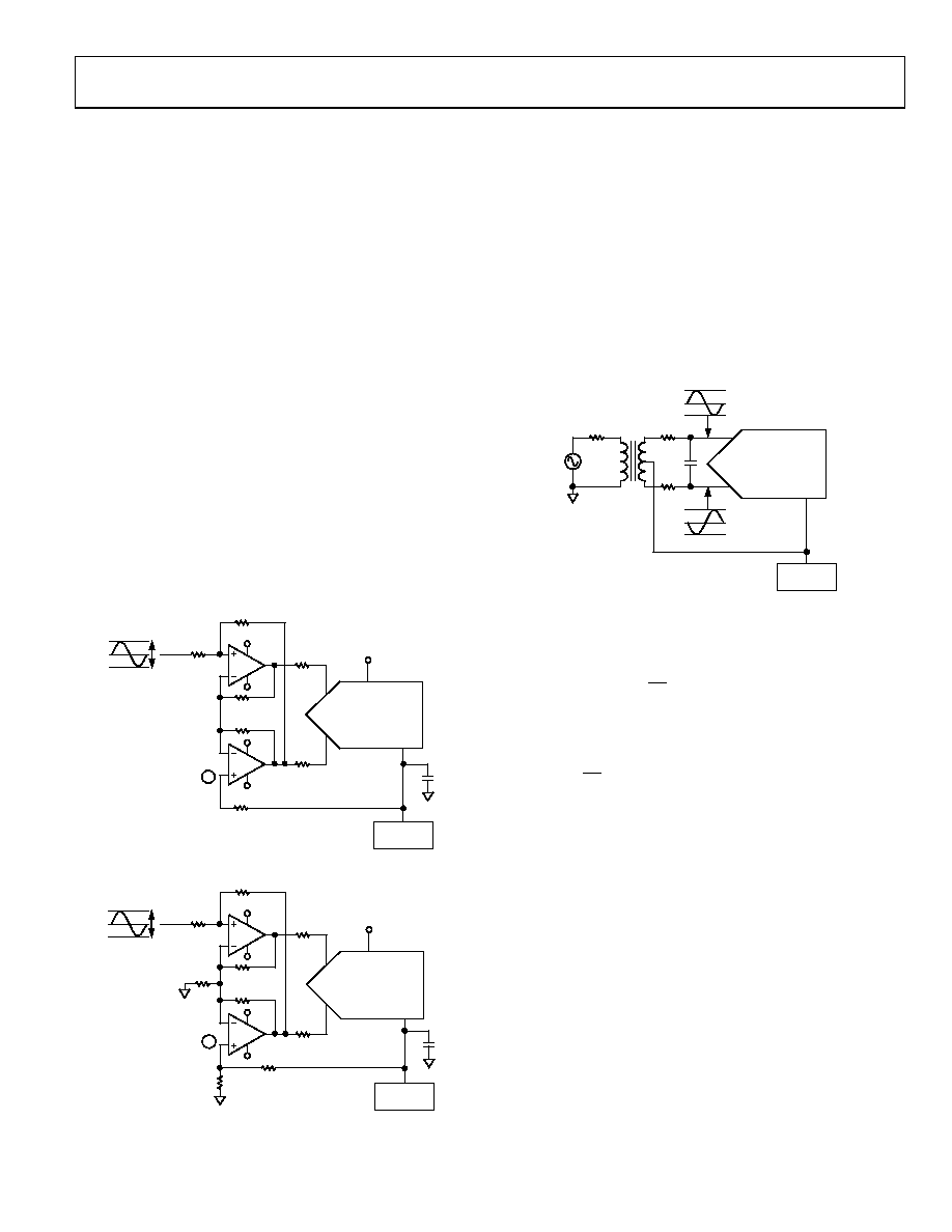
RF Transformer
An RF transformer with a center tap offers a good solution for
generating differential inputs in systems that do not need to
be dc-coupled. Figure 37 shows how a transformer is used for
single-ended-to-differential conversion. It provides the benefits
of operating the ADC in the differential mode without contri-
buting additional noise and distortion. An RF transformer also
has the benefit of providing electrical isolation between the
signal source and the ADC. A transformer can be used for most
ac applications. The center tap is used to shift the differential
signal to the common-mode level required; in this case, it is
connected to the reference so the common-mode level is the
value of the reference.
03051-A
-037
R
C
3.75V
2.5V
1.25V
3.75V
2.5V
1.25V
R
VIN+
VIN–
VREF
AD7440/
AD7450A
EXTERNAL
VREF
Figure 37. Using an RF Transformer to Generate Differential Inputs
DIGITAL INPUTS
The digital inputs applied to the device are not limited by the
maximum ratings, which limit the analog limits. Instead the
digital inputs applied, CS and SCLK, can go to 7 V and are not
restricted by the VDD + 0.3 V limits as on the analog input.
The main advantage of the inputs not being restricted to the
VDD + 0.3 V limit is that power supply sequencing issues are
avoided. If CS and SCLK are applied before VDD, there is no risk
of latch-up as there would be on the analog inputs if a signal
greater than 0.3 V was applied prior to VDD.
REFERENCE
An external reference source is required to supply the reference
to the device. This reference input can range from 100 mV to
3.5 V. With a 5 V power supply, the specified reference is 2.5 V
and the maximum reference is 3.5 V. With a 3 V power supply,
the specified reference is 2 V and the maximum reference is
2.2 V. In both cases, the reference is functional from 100 mV.
Ensure that, when choosing the reference value for a particular
application, the maximum analog input range (VIN max) is
never greater than VDD + 0.3 V to comply with the maximum
ratings of the device. The following two examples calculate the
maximum VREF input that can be used when operating the
AD7440/AD7450A at a VDD of 5 V and 3 V, respectively.
相关PDF资料 |
PDF描述 |
|---|---|
| MS27473P14B5S | CONN PLUG 5POS STRAIGHT W/SCKT |
| AD7993BRU-0 | IC ADC 10BIT 4CH W/I2C 16-TSSOP |
| MS27473E8B6SA | CONN PLUG 6POS STRAIGHT W/SCKT |
| LTC1863LCGN#TRPBF | IC ADC 12BIT 8CH 175KSPS 16SSOP |
| LTC2309CF#PBF | IC ADC 12BIT SAR 20-TSSOP |
相关代理商/技术参数 |
参数描述 |
|---|---|
| AD7440BRTZ-R22 | 制造商:AD 制造商全称:Analog Devices 功能描述:Differential Input, 1 MSPS ADCs in an 8-Lead SOT-23 |
| AD7440BRTZ-REEL7 | 功能描述:IC ADC 10BIT DIFF 1MSPS SOT23-8 RoHS:是 类别:集成电路 (IC) >> 数据采集 - 模数转换器 系列:- 标准包装:2,500 系列:- 位数:16 采样率(每秒):15 数据接口:MICROWIRE?,串行,SPI? 转换器数目:1 功率耗散(最大):480µW 电压电源:单电源 工作温度:-40°C ~ 85°C 安装类型:表面贴装 封装/外壳:38-WFQFN 裸露焊盘 供应商设备封装:38-QFN(5x7) 包装:带卷 (TR) 输入数目和类型:16 个单端,双极;8 个差分,双极 配用:DC1011A-C-ND - BOARD DELTA SIGMA ADC LTC2494 |
| AD7440BRTZ-REEL72 | 制造商:AD 制造商全称:Analog Devices 功能描述:Differential Input, 1 MSPS ADCs in an 8-Lead SOT-23 |
| AD7441 | 制造商:AD 制造商全称:Analog Devices 功能描述:Pseudo Differential, 1MSPS, 12- & 10-Bit ADCs in 8-lead SOT-23 |
| AD7441_10 | 制造商:AD 制造商全称:Analog Devices 功能描述:Pseudo Differential Input, 1 MSPS, 10-/12-Bit ADCs in an 8-Lead SOT-23 |
发布紧急采购,3分钟左右您将得到回复。