- 您现在的位置:买卖IC网 > PDF目录10322 > AD7440BRTZ-R2 (Analog Devices Inc)IC ADC 10BIT W/DIFF INP SOT-23-8 PDF资料下载
参数资料
| 型号: | AD7440BRTZ-R2 |
| 厂商: | Analog Devices Inc |
| 文件页数: | 9/29页 |
| 文件大小: | 0K |
| 描述: | IC ADC 10BIT W/DIFF INP SOT-23-8 |
| 标准包装: | 1 |
| 位数: | 10 |
| 采样率(每秒): | 1M |
| 数据接口: | DSP,MICROWIRE?,QSPI?,串行,SPI? |
| 转换器数目: | 1 |
| 功率耗散(最大): | 9.25mW |
| 电压电源: | 单电源 |
| 工作温度: | -40°C ~ 85°C |
| 安装类型: | 表面贴装 |
| 封装/外壳: | SOT-23-8 |
| 供应商设备封装: | SOT-23-8 |
| 包装: | 标准包装 |
| 输入数目和类型: | 1 个差分,单极 |
| 其它名称: | AD7440BRTZ-R2DKR |
第1页第2页第3页第4页第5页第6页第7页第8页当前第9页第10页第11页第12页第13页第14页第15页第16页第17页第18页第19页第20页第21页第22页第23页第24页第25页第26页第27页第28页第29页
AD7440/AD7450A
Rev. C | Page 16 of 28
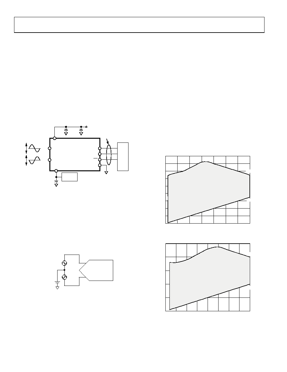
TYPICAL CONNECTION DIAGRAM
Figure 26 shows a typical connection diagram for the
AD7440/AD7450A for both 5 V and 3 V supplies. In this setup,
the GND pin is connected to the analog ground plane of the
system. The VREF pin is connected to either a 2.5 V or a 2 V
decoupled reference source, depending on the power supply, to
set up the analog input range. The common-mode voltage has
to be set up externally and is the value on which the two inputs
are centered. The conversion result is output in a 16-bit word
with four leading zeros followed by the MSB of the 12-bit or
10-bit result. The 10-bit result of the AD7440 is followed by two
trailing zeros. For more details on driving the differential inputs
and setting up the common mode, refer to the Driving
Differential Inputs section.
03051-A
-026
AD7440/
AD7450A
0.1
μF
0.1
μF
10
μF
VREF
VDD
VIN+
SCLK
3V/5V
SUPPLY
SERIAL
INTERFACE
μC/μP
SDATA
CS
GND
VIN–
2V/2.5V
VREF
*CM IS THE COMMON-MODE VOLTAGE.
CM*
VREF
p-p
CM*
VREF
p-p
Figure 26. Typical Connection Diagram
ANALOG INPUT
The analog input of the AD7440/AD7450A is fully differential.
Differential signals have a number of benefits over single-
ended signals, including noise immunity based on the device’s
common-mode rejection, improvements in distortion perfor-
mance, doubling of the device’s available dynamic range, and
flexibility in input ranges and bias points. Figure 27 defines the
fully differential analog input of the AD7440/AD7450A.
03051-A
-027
VREF
p-p
VIN+
VIN–
VREF
p-p
AD7440/
AD7450A
COMMON-MODE
VOLTAGE
Figure 27. Differential Input Definitions
The amplitude of the differential signal is the difference
between the signals applied to the VIN+ and VIN– pins
(i.e., VIN+ – VIN–). VIN+ and VIN– are simultaneously driven by
two signals each of amplitude VREF that are 180° out of phase.
The amplitude of the differential signal is therefore –VREF to
+VREF peak-to-peak (2 × VREF). This is true regardless of the
common mode (CM).
The common mode is the average of the two signals, that is,
(VIN+ + VIN–)/2 and is therefore the voltage that the two inputs
are centered on. This results in the span of each input being
CM ± VREF/2. This voltage has to be set up externally, and its
range varies with VREF. As the value of VREF increases, the
common-mode range decreases. When driving the inputs with
an amplifier, the actual common-mode range is determined by
the amplifier’s output voltage swing.
typically varies with VREF for both a 5 V and a 3 V power supply.
The common mode must be in this range to guarantee the
functionality of the AD7440/AD7450A.
For ease of use, the common mode can be set up to equal VREF,
resulting in the differential signal being ±VREF centered on VREF.
When a conversion takes place, the common mode is rejected,
resulting in a virtually noise-free signal of amplitude –VREF to
+VREF, corresponding to the digital codes of 0 to 4096 in the
case of the AD7450A and 0 to 1024 in the AD7440.
4.5
4.0
3.5
3.0
2.5
2.0
1.5
1.0
0.5
0
0.5
1.0
1.5
2.0
2.5
3.0
3.5
03051-A
-028
VREF (V)
COMMON-MODE
V
O
LTAGE
(V
)
1.75V
3.25V
COMMON-MODE RANGE
Figure 28. Input Common-Mode Range vs. VREF
(VDD = 5 V and VREF (Max) = 3.5 V)
2.5
0.5
1.0
1.5
2.0
0
0.25
0.50
0.75
1.00
1.25
1.50
1.75
2.00
03051-A
-029
VREF (V)
COMMON-MODE
V
O
LTAGE
(V
)
1V
2V
COMMON-MODE RANGE
Figure 29. Input Common-Mode Range vs. VREF
(VDD = 3 V and VREF (Max) =2V)
相关PDF资料 |
PDF描述 |
|---|---|
| MS27473P14B5S | CONN PLUG 5POS STRAIGHT W/SCKT |
| AD7993BRU-0 | IC ADC 10BIT 4CH W/I2C 16-TSSOP |
| MS27473E8B6SA | CONN PLUG 6POS STRAIGHT W/SCKT |
| LTC1863LCGN#TRPBF | IC ADC 12BIT 8CH 175KSPS 16SSOP |
| LTC2309CF#PBF | IC ADC 12BIT SAR 20-TSSOP |
相关代理商/技术参数 |
参数描述 |
|---|---|
| AD7440BRTZ-R22 | 制造商:AD 制造商全称:Analog Devices 功能描述:Differential Input, 1 MSPS ADCs in an 8-Lead SOT-23 |
| AD7440BRTZ-REEL7 | 功能描述:IC ADC 10BIT DIFF 1MSPS SOT23-8 RoHS:是 类别:集成电路 (IC) >> 数据采集 - 模数转换器 系列:- 标准包装:2,500 系列:- 位数:16 采样率(每秒):15 数据接口:MICROWIRE?,串行,SPI? 转换器数目:1 功率耗散(最大):480µW 电压电源:单电源 工作温度:-40°C ~ 85°C 安装类型:表面贴装 封装/外壳:38-WFQFN 裸露焊盘 供应商设备封装:38-QFN(5x7) 包装:带卷 (TR) 输入数目和类型:16 个单端,双极;8 个差分,双极 配用:DC1011A-C-ND - BOARD DELTA SIGMA ADC LTC2494 |
| AD7440BRTZ-REEL72 | 制造商:AD 制造商全称:Analog Devices 功能描述:Differential Input, 1 MSPS ADCs in an 8-Lead SOT-23 |
| AD7441 | 制造商:AD 制造商全称:Analog Devices 功能描述:Pseudo Differential, 1MSPS, 12- & 10-Bit ADCs in 8-lead SOT-23 |
| AD7441_10 | 制造商:AD 制造商全称:Analog Devices 功能描述:Pseudo Differential Input, 1 MSPS, 10-/12-Bit ADCs in an 8-Lead SOT-23 |
发布紧急采购,3分钟左右您将得到回复。