- 您现在的位置:买卖IC网 > PDF目录10543 > AD7475ARZ (Analog Devices Inc)IC ADC 12BIT SERIAL LP 8SOIC PDF资料下载
参数资料
| 型号: | AD7475ARZ |
| 厂商: | Analog Devices Inc |
| 文件页数: | 10/25页 |
| 文件大小: | 0K |
| 描述: | IC ADC 12BIT SERIAL LP 8SOIC |
| 标准包装: | 98 |
| 位数: | 12 |
| 采样率(每秒): | 1M |
| 数据接口: | DSP,MICROWIRE?,QSPI?,串行,SPI? |
| 转换器数目: | 1 |
| 功率耗散(最大): | 10.5mW |
| 电压电源: | 单电源 |
| 工作温度: | -40°C ~ 85°C |
| 安装类型: | 表面贴装 |
| 封装/外壳: | 8-SOIC(0.154",3.90mm 宽) |
| 供应商设备封装: | 8-SOIC |
| 包装: | 管件 |
| 输入数目和类型: | 1 个单端,单极 |
AD7475/AD7495
Rev. B | Page 17 of 24
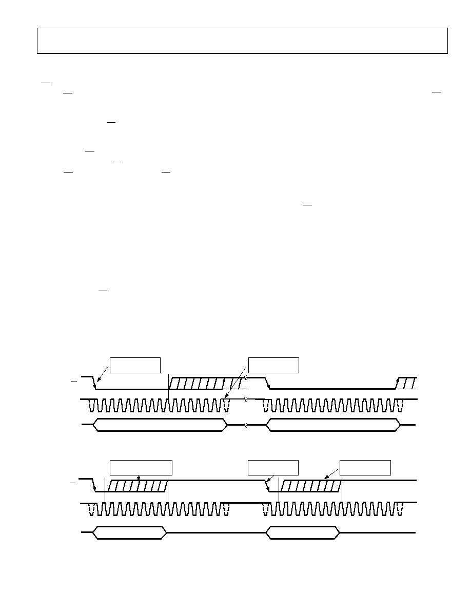
To exit this operating mode and power up the AD7475/AD7495
again, a dummy conversion is performed. On the falling edge of
CS, the device begins to power up and continues to power up as
long as CS is held low until after the falling edge of the tenth
SCLK. The device is fully powered up once 16 SCLKs have
elapsed, and valid data results from the next conversion, as
shown in Figure 21. If CS is brought high before the second
falling edge of SCLK, the AD7475/AD7495 go back into partial
power-down again. This avoids accidental power-up due to
glitches on the CS line; although the device may begin to power
up on the falling edge of CS, it powers down again on the rising
edge of CS. If in partial power-down and CS is brought high
between the second and tenth falling edges of SCLK, the device
enters full power-down mode.
Power-Up Time
The power-up time of the AD7475/AD7495 from partial
power-down is typically 1 μs, which means that with any
frequency of SCLK up to 20 MHz, one dummy cycle is
sufficient to allow the device to power up from partial power-
down. Once the dummy cycle is complete, the ADC is fully
powered up and the input signal is acquired properly. The quiet
time, tQUIET, must still be allowed from the point where the bus
goes back into three-state after the dummy conversion to the
next falling edge of CS. When running at a 1 MSPS throughput
rate, the AD7475/AD7495 power up and acquire a signal within
±0.5 LSB in one dummy cycle, 1 μs.
When powering up from the power-down mode with a dummy
cycle, as in Figure 21, the track-and-hold that was in hold mode
while the part was powered down returns to track mode after
the first SCLK edge the part receives after the falling edge of CS.
This is shown as Point A in Figure 21. Although at any SCLK
frequency one dummy cycle is sufficient to power up the device
and acquire VIN, it does not necessarily mean that a full dummy
cycle of 16 SCLKs must always elapse to power up the device
and fully acquire VIN; 1 μs is sufficient to power up the device
and acquire the input signal. If, for example, a 5 MHz SCLK
frequency were applied to the ADC, the cycle time would be
3.2 μs. In one dummy cycle, 3.2 μs, the part would be powered
up and VIN fully acquired. However, after 1 μs with a 5 MHz
SCLK, only 5 SCLK cycles would have elapsed. At this stage,
the ADC would be fully powered up and the signal acquired.
In this case, the CS can be brought high after the tenth SCLK
falling edge and brought low again after a time, tQUIET, to initiate
the conversion.
FULL POWER-DOWN MODE
Full power-down mode is intended for use in applications
where slower throughput rates are required than that in the
partial power-down mode, because power up from a full power-
down would not be complete in just one dummy conversion.
This mode is more suited to applications where a series of
conversions performed at a relatively high throughput rate are
followed by a long period of inactivity and therefore power
down. When the AD7475/AD7495 are in full power-down, all
analog circuitry is powered down.
SCLK
SDATA
INVALID DATA
VALID DATA
1
10
16
1
THE PART BEGINS
TO POWER UP
THE PART IS FULLY
POWERED UP
16
A
CS
01684-B
-021
Figure 21. Exiting Partial Power-Down Mode
SCLK
SDATA
INVALID DATA
1
10
16
1
THE PART BEGINS
TO POWER UP
16
2
10
2
THE PART ENTERS
FULL POWER-DOWN
THE PART ENTERS
PARTIAL POWER-DOWN
THREE-STATE
01684-B
-023
CS
Figure 22. Entering Full Power-Down Mode
相关PDF资料 |
PDF描述 |
|---|---|
| VE-J4P-MW-F1 | CONVERTER MOD DC/DC 13.8V 100W |
| AD7451ARMZ | IC ADC 12BIT DIFF 1MSPS 8MSOP |
| AD7705BNZ | IC ADC 16BIT 2CH 16-DIP |
| VE-J4N-MW-F4 | CONVERTER MOD DC/DC 18.5V 100W |
| AD7887BRZ | IC ADC 12BIT 2CHAN SRL 8SOIC |
相关代理商/技术参数 |
参数描述 |
|---|---|
| AD7475BR | 功能描述:IC ADC 12BIT SRL LP 8-SOIC RoHS:否 类别:集成电路 (IC) >> 数据采集 - 模数转换器 系列:- 标准包装:1,000 系列:- 位数:12 采样率(每秒):300k 数据接口:并联 转换器数目:1 功率耗散(最大):75mW 电压电源:单电源 工作温度:0°C ~ 70°C 安装类型:表面贴装 封装/外壳:24-SOIC(0.295",7.50mm 宽) 供应商设备封装:24-SOIC 包装:带卷 (TR) 输入数目和类型:1 个单端,单极;1 个单端,双极 |
| AD7475BRM | 功能描述:IC ADC 12BIT SRL LP 8-MSOP RoHS:否 类别:集成电路 (IC) >> 数据采集 - 模数转换器 系列:- 产品培训模块:Lead (SnPb) Finish for COTS Obsolescence Mitigation Program 标准包装:2,500 系列:- 位数:12 采样率(每秒):3M 数据接口:- 转换器数目:- 功率耗散(最大):- 电压电源:- 工作温度:- 安装类型:表面贴装 封装/外壳:SOT-23-6 供应商设备封装:SOT-23-6 包装:带卷 (TR) 输入数目和类型:- |
| AD7475BRM-REEL | 制造商:Analog Devices 功能描述:ADC Single SAR 1Msps 12-bit Serial 8-Pin MSOP T/R 制造商:Analog Devices 功能描述:ADC SGL SAR 1MSPS 12-BIT SERL 8MSOP - Tape and Reel 制造商:Rochester Electronics LLC 功能描述:FAST 12-BIT LOW POWER SERIAL ADC I.C. - Tape and Reel |
| AD7475BRM-REEL7 | 功能描述:IC ADC 12BIT SRL LP 8-MSOP T/R RoHS:否 类别:集成电路 (IC) >> 数据采集 - 模数转换器 系列:- 标准包装:1,000 系列:- 位数:16 采样率(每秒):45k 数据接口:串行 转换器数目:2 功率耗散(最大):315mW 电压电源:模拟和数字 工作温度:0°C ~ 70°C 安装类型:表面贴装 封装/外壳:28-SOIC(0.295",7.50mm 宽) 供应商设备封装:28-SOIC W 包装:带卷 (TR) 输入数目和类型:2 个单端,单极 |
| AD7475BRMZ | 功能描述:IC ADC 12BIT SERIAL LP 8MSOP RoHS:是 类别:集成电路 (IC) >> 数据采集 - 模数转换器 系列:- 其它有关文件:TSA1204 View All Specifications 标准包装:1 系列:- 位数:12 采样率(每秒):20M 数据接口:并联 转换器数目:2 功率耗散(最大):155mW 电压电源:模拟和数字 工作温度:-40°C ~ 85°C 安装类型:表面贴装 封装/外壳:48-TQFP 供应商设备封装:48-TQFP(7x7) 包装:Digi-Reel® 输入数目和类型:4 个单端,单极;2 个差分,单极 产品目录页面:1156 (CN2011-ZH PDF) 其它名称:497-5435-6 |
发布紧急采购,3分钟左右您将得到回复。