参数资料
| 型号: | AD7609BSTZ-RL |
| 厂商: | Analog Devices Inc |
| 文件页数: | 26/36页 |
| 文件大小: | 0K |
| 描述: | IC DAS W/ADC 18BIT 8CH 64LQFP |
| 标准包装: | 1,500 |
| 类型: | 数据采集系统(DAS),ADC |
| 分辨率(位): | 18 b |
| 采样率(每秒): | 200k |
| 数据接口: | DSP,MICROWIRE?,并联,QSPI?,串行,SPI? |
| 电压电源: | 模拟和数字 |
| 电源电压: | 2.3 V ~ 5 V,4.75 V ~ 5.25 V |
| 工作温度: | -40°C ~ 85°C |
| 安装类型: | 表面贴装 |
| 封装/外壳: | 64-LQFP |
| 供应商设备封装: | 64-LQFP(10x10) |
| 包装: | 带卷 (TR) |
第1页第2页第3页第4页第5页第6页第7页第8页第9页第10页第11页第12页第13页第14页第15页第16页第17页第18页第19页第20页第21页第22页第23页第24页第25页当前第26页第27页第28页第29页第30页第31页第32页第33页第34页第35页第36页
AD7609
Data Sheet
Rev. A | Page 32 of 36
LAYOUT GUIDELINES
The printed circuit board that houses the AD7609 should be
designed so that the analog and digital sections are separated
and confined to different areas of the board.
Use at least one ground plane. It can be common or split
between the digital and analog sections. In the case of the split
plane, the digital and analog ground planes should be joined in
only one place, preferably as close as possible to the AD7609.
If the AD7609 is in a system where multiple devices require
analog-to-digital ground connections, the connection should
still be made at only one point, a star ground point, which
should be established as close as possible to the AD7609. Good
connections should be made to the ground plane. Avoid sharing
one connection for multiple ground pins. Individual vias or
multiple vias to the ground plane should be used for each
ground pin.
Avoid running digital lines under the devices because doing
so couples noise onto the die. Allow the analog ground plane
to run under the AD7609 to avoid noise coupling. Shield fast-
switching signals like CONVST A, CONVST B, or clocks with
digital ground to avoid radiating noise to other sections of the
board, and they should never run near analog signal paths.
Avoid crossover of digital and analog signals. Run traces on
layers in close proximity on the board at right angles to each
other to reduce the effect of feedthrough through the board.
The power supply lines to the AVCC and VDRIVE pins on the
AD7609 should use as large a trace as possible to provide low
impedance paths and reduce the effect of glitches on the power
supply lines. Where possible, use supply planes. Good connec-
tions should be made between the AD7609 supply pins and the
power tracks on the board; this should involve the use of a single
via or multiple vias for each supply pin.
Good decoupling is also important to lower the supply imped-
ance presented to the AD7609 and to reduce the magnitude of
the supply spikes. Place the decoupling capacitors close to,
ideally right up against, these pins and their corresponding
ground pins. Place the decoupling capacitors for the REFIN/
REFOUT pin and the REFCAPA and REFCAPB pins as close as
possible to their respective AD7609 pins. Where possible, they
should be placed on the same side of the board as the AD7609
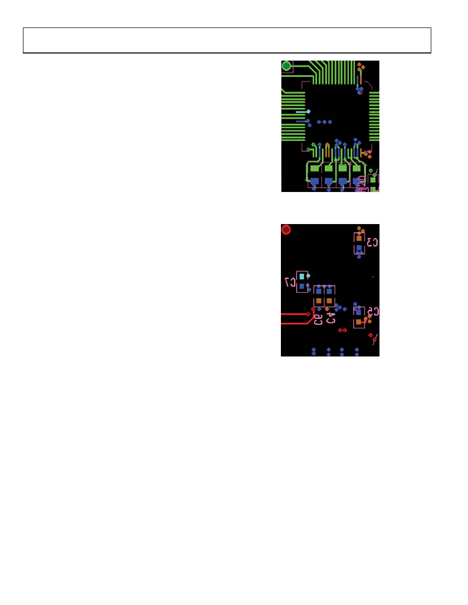
device. Figure 60 shows the recommended decoupling on the
top layer of the AD7609 board. Figure 61 shows bottom layer
decoupling. Bottom layer decoupling is for the four AVCC pins
and the VDRIVE pin.
09760-
057
Figure 60. Top Layer Decoupling REFIN/REFOUT, REFCAPA, REFCAPB, and
REGCAP Pins
09760-
058
Figure 61. Bottom Layer Decoupling
相关PDF资料 |
PDF描述 |
|---|---|
| AD760AQ | IC DAC 16BIT W/AMP SRL 28-CDIP |
| AD766AN | IC DAC 16BIT W/REF DSP 16-DIP |
| AD767BD | IC DAC 12BIT W/AMP 24-CDIP |
| AD768AR | IC DAC 16BIT 30MSPS 28-SOIC |
| AD7724ASTZ | IC MOD SIGMA-DELTA DUAL 48LQFP |
相关代理商/技术参数 |
参数描述 |
|---|---|
| AD760AN | 制造商:未知厂家 制造商全称:未知厂家 功能描述:16-Bit Digital-to-Analog Converter |
| AD760AP | 制造商:未知厂家 制造商全称:未知厂家 功能描述:16-Bit Digital-to-Analog Converter |
| AD760AQ | 功能描述:IC DAC 16BIT W/AMP SRL 28-CDIP RoHS:否 类别:集成电路 (IC) >> 数据采集 - 数模转换器 系列:DACPORT® 产品培训模块:Lead (SnPb) Finish for COTS Obsolescence Mitigation Program 标准包装:50 系列:- 设置时间:4µs 位数:12 数据接口:串行 转换器数目:2 电压电源:单电源 功率耗散(最大):- 工作温度:-40°C ~ 85°C 安装类型:表面贴装 封装/外壳:8-TSSOP,8-MSOP(0.118",3.00mm 宽) 供应商设备封装:8-uMAX 包装:管件 输出数目和类型:2 电压,单极 采样率(每秒):* 产品目录页面:1398 (CN2011-ZH PDF) |
| AD760SQ | 制造商:未知厂家 制造商全称:未知厂家 功能描述:16-Bit Digital-to-Analog Converter |
| AD7610 | 制造商:AD 制造商全称:Analog Devices 功能描述:14-Bit, 1 MSPS, Differential, Programmable Input PulSAR ADC |
发布紧急采购,3分钟左右您将得到回复。