- 您现在的位置:买卖IC网 > PDF目录165343 > AD7609BSTZ (ANALOG DEVICES INC) 8-CH 18-BIT SUCCESSIVE APPROXIMATION ADC, SERIAL/PARALLEL ACCESS, PQFP64 PDF资料下载
参数资料
| 型号: | AD7609BSTZ |
| 厂商: | ANALOG DEVICES INC |
| 元件分类: | ADC |
| 英文描述: | 8-CH 18-BIT SUCCESSIVE APPROXIMATION ADC, SERIAL/PARALLEL ACCESS, PQFP64 |
| 封装: | ROHS COMPLIANT, MS-026BCD, LQFP-64 |
| 文件页数: | 15/35页 |
| 文件大小: | 1737K |
| 代理商: | AD7609BSTZ |
第1页第2页第3页第4页第5页第6页第7页第8页第9页第10页第11页第12页第13页第14页当前第15页第16页第17页第18页第19页第20页第21页第22页第23页第24页第25页第26页第27页第28页第29页第30页第31页第32页第33页第34页第35页
AD7609
Preliminary Technical Data
Rev. PrD | Page 22 of 35
THEORY OF OPERATION
CONVERTER DETAILS
The AD7609 is a data acquisition system that employs a high
speed, low power, charge redistribution successive approxima-
tion analog-to-digital converter (ADC) and allows the
simultaneous sampling of eight true differential analog input
channels. The analog inputs on the AD7609 can accept true
bipolar input signals. The RANGE pin is used to select either
±10 V or ±5 V as the input range. The AD7609 operates from
a single 5 V supply.
The AD7609 contains input clamp protection, input signal
scaling amplifiers, second-order antialiasing filter, track-and-
hold amplifiers, an on-chip reference, reference buffers, a high
speed ADC, digital filter and high speed parallel and serial
interfaces. Sampling on the AD7609 is controlled using
CONVST x signals.
ANALOG INPUT
Analog Input Ranges
The AD7609 can handle true bipolar input voltages. The logic
level on the RANGE pin determines the analog input range of
all analog input channels. If this pin is tied to a logic high, the
analog input range is ±10 V for all channels. If this pin is tied
to a logic low, the analog input range is ±5 V for all channels.
A logic change on this pin has an immediate effect on the
analog input range; however, there will be a settling time of
80 μs typically, in addition to the normal acquisition time
requirement. The recommended practice is to hardwire the
RANGE pin according to the desired input range for the system
signals.
Analog Input Impedance
The analog input impedance of the AD7609 is 1 MΩ. This is a
fixed input impedance and does not vary with the AD7609 sam-
pling frequency. This high analog input impedance eliminates
the need for a driver amplifier in front of the AD7609 allowing
for direct connection to the source or sensor. With the need for
a driver amplifier eliminated, bipolar supplies can be removed
from the signal chain, which are often a source of noise in a
system.
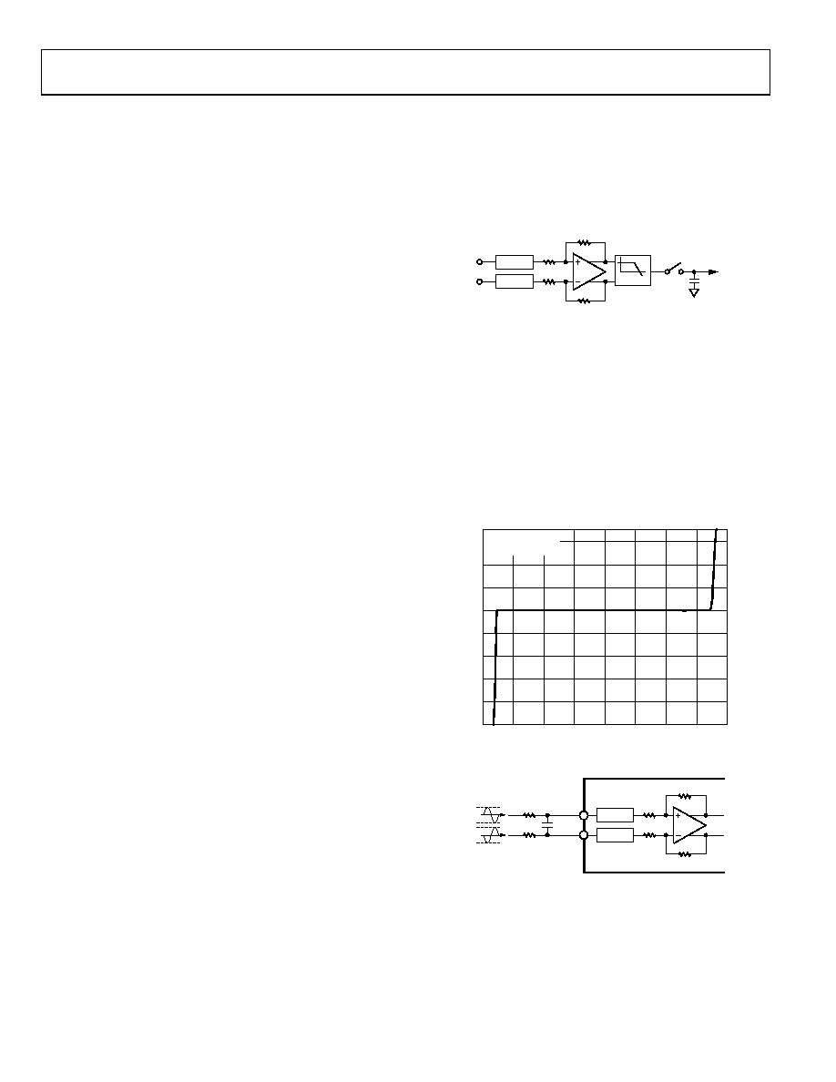
Analog Input Clamp Protection
Figure 33 shows the analog input structure of the AD7609.
Each AD7609 analog input contains clamp protection circuitry.
Despite a single 5 V supply operation, this analog input clamp
protection allows for an input over voltage up to ±16.5 V.
1M
CLAMP
Vx+
1M
CLAMP
Vx–
SECOND-
ORDER
LPF
RFB
09
76
0
-12
9
Figure 33. Analog Input Circuitry
Figure 34 shows the voltage vs. current characteristic of the
clamp circuit. For input voltages up to ±16.5 V, no current flows
in the clamp circuit. For input voltages above ±16.5 V the
AD7609 clamp circuitry turns on and clamps the analog input
to ±16.5 V. A series resister should be placed on the analog
input channels to limit the current to ±10 mA for input voltages
above ±16.5 V. In an application where there is a series
resistance on an analog input channel VINx+, a corresponding
resistance is required on the VINx channel, see Figure 35. If
there is no corresponding resister on the Vx channel, this will
result in a gain error on that channel.
30
–50
–40
–30
–20
–10
0
10
20
–20
–15
–10
–5
0
5
10
15
20
IN
P
UT
C
L
AM
P
CUR
RE
NT
(
m
A)
SOURCE VOLTAGE (V)
08
47
9-
0
33
AVCC, VDRIVE = 5V
TA = 25°C
Figure 34. Input Protection Clamp Profile
1M
CLAMP
VINx+
1M
CLAMP
VINx–
RFB
C
R
+10V
–10V
AD7609
09
76
0-
0
31
+10V
–10V
Figure 35. Input Resistance Matching on the Analog Input
相关PDF资料 |
PDF描述 |
|---|---|
| AD7746 | DIGITAL TEMP SENSOR-SERIAL, 24BIT(s), 2Cel, RECTANGULAR, SURFACE MOUNT |
| AD7811YRUZ | 4-CH 10-BIT SUCCESSIVE APPROXIMATION ADC, SERIAL ACCESS, PDSO16 |
| AD7845KRZ | PARALLEL, WORD INPUT LOADING, 2.5 us SETTLING TIME, 12-BIT DAC, PDSO24 |
| AD7911ARMZ-REEL | 2-CH 10-BIT SUCCESSIVE APPROXIMATION ADC, SERIAL ACCESS, PDSO8 |
| AD7911AUJZ-R2 | 2-CH 10-BIT SUCCESSIVE APPROXIMATION ADC, SERIAL ACCESS, PDSO8 |
相关代理商/技术参数 |
参数描述 |
|---|---|
| AD7609BSTZ-RL | 功能描述:IC DAS W/ADC 18BIT 8CH 64LQFP RoHS:是 类别:集成电路 (IC) >> 数据采集 - ADCs/DAC - 专用型 系列:- 产品培训模块:Lead (SnPb) Finish for COTS Obsolescence Mitigation Program 标准包装:50 系列:- 类型:数据采集系统(DAS) 分辨率(位):16 b 采样率(每秒):21.94k 数据接口:MICROWIRE?,QSPI?,串行,SPI? 电压电源:模拟和数字 电源电压:1.8 V ~ 3.6 V 工作温度:-40°C ~ 85°C 安装类型:表面贴装 封装/外壳:40-WFQFN 裸露焊盘 供应商设备封装:40-TQFN-EP(6x6) 包装:托盘 |
| AD760AN | 制造商:未知厂家 制造商全称:未知厂家 功能描述:16-Bit Digital-to-Analog Converter |
| AD760AP | 制造商:未知厂家 制造商全称:未知厂家 功能描述:16-Bit Digital-to-Analog Converter |
| AD760AQ | 功能描述:IC DAC 16BIT W/AMP SRL 28-CDIP RoHS:否 类别:集成电路 (IC) >> 数据采集 - 数模转换器 系列:DACPORT® 产品培训模块:Lead (SnPb) Finish for COTS Obsolescence Mitigation Program 标准包装:50 系列:- 设置时间:4µs 位数:12 数据接口:串行 转换器数目:2 电压电源:单电源 功率耗散(最大):- 工作温度:-40°C ~ 85°C 安装类型:表面贴装 封装/外壳:8-TSSOP,8-MSOP(0.118",3.00mm 宽) 供应商设备封装:8-uMAX 包装:管件 输出数目和类型:2 电压,单极 采样率(每秒):* 产品目录页面:1398 (CN2011-ZH PDF) |
| AD760SQ | 制造商:未知厂家 制造商全称:未知厂家 功能描述:16-Bit Digital-to-Analog Converter |
发布紧急采购,3分钟左右您将得到回复。