参数资料
| 型号: | AD760AQ |
| 厂商: | Analog Devices Inc |
| 文件页数: | 11/12页 |
| 文件大小: | 0K |
| 描述: | IC DAC 16BIT W/AMP SRL 28-CDIP |
| 产品培训模块: | Data Converter Fundamentals DAC Architectures |
| 标准包装: | 1 |
| 系列: | DACPORT® |
| 设置时间: | 6µs |
| 位数: | 16 |
| 数据接口: | 串行,并联 |
| 转换器数目: | 1 |
| 电压电源: | 双 ± |
| 功率耗散(最大): | 725mW |
| 工作温度: | -40°C ~ 85°C |
| 安装类型: | 通孔 |
| 封装/外壳: | 28-CDIP(0.600",15.24mm) |
| 供应商设备封装: | 28-CDIP |
| 包装: | 管件 |
| 输出数目和类型: | 2 电压,单极;2 电压,双极 |
| 采样率(每秒): | 167k |
| 产品目录页面: | 781 (CN2011-ZH PDF) |
–8–
AD760
REV. A
SPAN/
BIP OFF
VOUT
23
24
25
MAIN DAC
REFOUT
26
REFI N
R1
50
10k
10k
9.95k
AD760
+10V REF
Figure 6a. 0 V to ±10 V Bipolar Voltage Output
Gain Error can be adjusted to zero using the circuit shown in
Figure 6b. Note that gain adjustment changes the Bipolar Zero
by one half of the variation made to the full-scale output value.
Therefore, to eliminate iterating between Zero (calibration) and
Gain adjustment the following procedure is recommended.
STEP 1 . . . ZERO ADJUST
Initiate Calibration Sequence.
STEP 2 . . . GAIN ADJUST
Insure the CALOK pin remains high throughout the gain ad-
justment process. Turn all bits on and measure the output error
relative to the full-scale output of 9.99695 V. Adjust R1 until
the output is minus two times the full-scale output error. For
example, if the output error is –1 mV, adjust the output 2 mV
higher than the previous full-scale error.
STEP 3 . . . ZERO ADJUST
Initiate Calibration Sequence. The AD760 will calibrate Bipolar
Zero and the resulting Gain Error will be very small. Reload the
DAC with all ones to check the full-scale output error.
SPAN/
BIP OFF
VOUT
23
24
+10V REF
25
MAIN DAC
REFOUT
26
REFI N
R1
100
10k
10k
9.95k
AD760
Figure 6b. 0 V to ±10 V Bipolar Voltage Output Gain
Adjustment
It should be noted that using external resistors will introduce a
small temperature drift component beyond that inherent in the
AD760. The internal resistors are trimmed to ratio-match and
temperature-track other resistors on chip, even though their
absolute tolerances are ±20% and absolute temperature coeffi-
cients are approximately –50 ppm/°C. In the case that external
resistors are used, the temperature coefficient mismatch be-
tween internal and external resistors, multiplied by the sensitiv-
ity of the circuit to variations in the external resistor value, will
be the resultant additional temperature drift.
INTERNAL/EXTERNAL REFERENCE USE
The AD760 has an internal low noise buried Zener diode refer-
ence that is trimmed for absolute accuracy and temperature co-
efficient. This reference is buffered and optimized for use in a
high speed DAC and will give long-term stability equal or supe-
rior to the best discrete Zener diode references. The perfor-
mance of the AD760 is specified with the internal reference
driving the DAC and with the DAC alone (for use with a preci-
sion external reference).
The internal reference has sufficient buffering to drive external
circuitry in addition to the reference currents required for the
DAC (typically 1 mA to REF IN and 1 mA to BIPOLAR OFF-
SET). A minimum of 2 mA is available for driving external
loads. The AD760 reference output should be buffered with an
external op amp if it is required to supply more than 4 mA total
current. The reference is tested and guaranteed to ±0.1% max
error.
It is also possible to use external references other than 10 volts
with slightly degraded linearity specifications. The recom-
mended range of reference voltages is +5 V to +10.24 V. For
example, by using the AD586 5 V reference, outputs of 0 V to
+5 V or ±5 V can be realized. Using the AD586 voltage refer-
ence makes it possible to operate the AD760 with ±12 V sup-
plies with 10% tolerances.
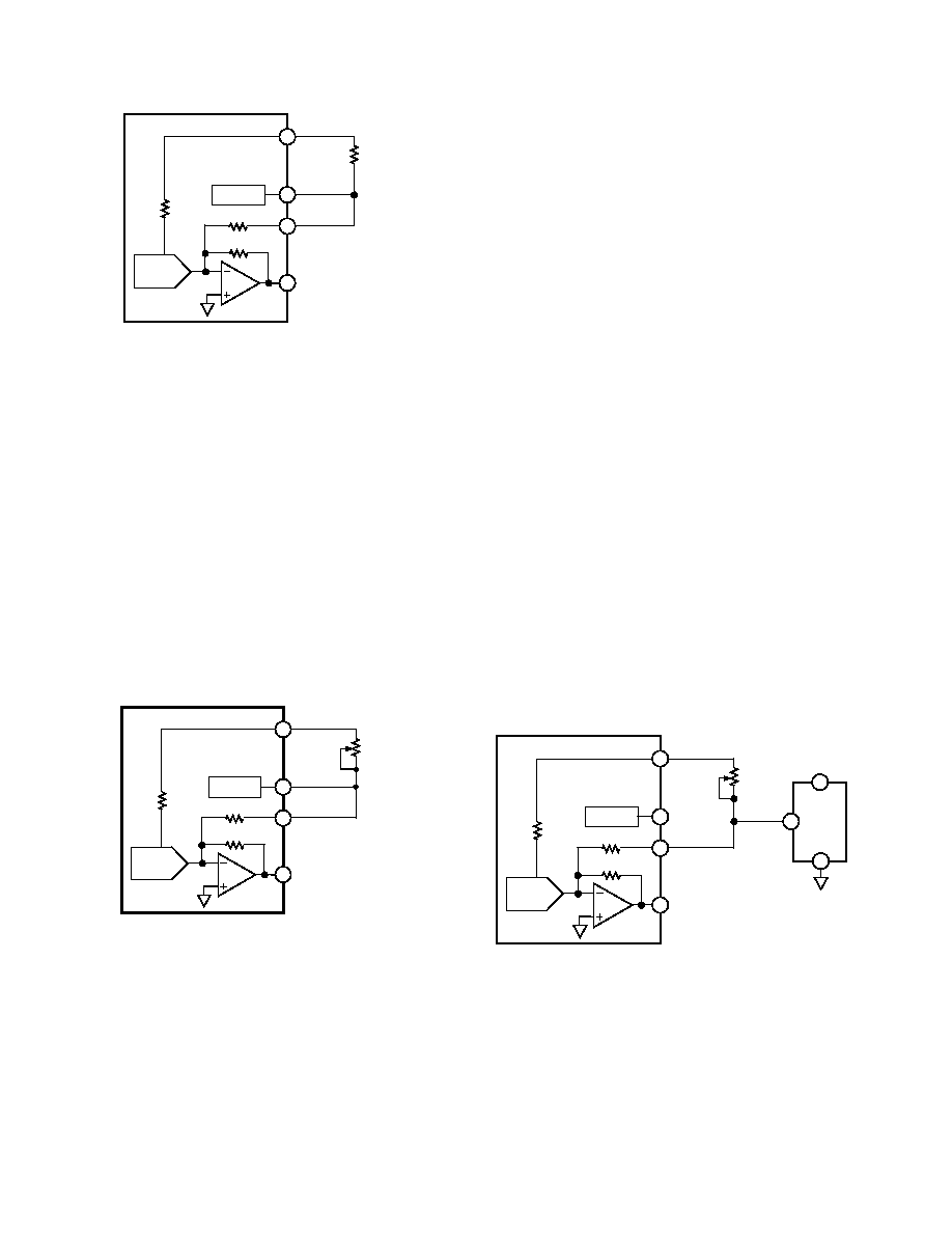
Figure 7 shows the AD760 using the AD586 precision 5 V refer-
ence in the bipolar configuration. The highest grade AD586MN
is specified with a drift of 2 ppm/°C. This circuit includes an
optional potentiometer that can be used to adjust the gain error
in a manner similar to that described in the Bipolar Configura-
tion section. Use +4.999847 V as the full-scale output value.
The AD760 can also be used with the AD587, 10 V reference,
using the same configuration shown in Figure 7 to produce a
±10 V output. The highest grade AD587L is specified at
5 ppm/°C.
SPAN/BIP OFF
VOUT
23
24
+10V REF
25
MAIN DAC
REFOUT
26
REFI N
100
10k
10k
9.95k
AD760
AD586
2
4
6
VOUT
+VCC
Figure 7. Using the AD760 with the AD586 5 V Reference
OUTPUT SETTLING AND GLITCH
The AD760’s output buffer amplifier typically settles to within
0.0008% FS (1/2 LSB) of its final value in 8 s for a full-scale
step. Figures 8a and 8b show settling for a full scale and an
LSB step, respectively, with a 2 k , 1000 pF load applied. The
guaranteed maximum settling time at +25°C for a full-scale step
is 13 s with this load. The typical settling time for a 1 LSB step
is 2.5 s.
相关PDF资料 |
PDF描述 |
|---|---|
| AD766AN | IC DAC 16BIT W/REF DSP 16-DIP |
| AD767BD | IC DAC 12BIT W/AMP 24-CDIP |
| AD768AR | IC DAC 16BIT 30MSPS 28-SOIC |
| AD7724ASTZ | IC MOD SIGMA-DELTA DUAL 48LQFP |
| AD7729ARU | IC ADC 15BIT DUAL W/DAC 28-TSSOP |
相关代理商/技术参数 |
参数描述 |
|---|---|
| AD760SQ | 制造商:未知厂家 制造商全称:未知厂家 功能描述:16-Bit Digital-to-Analog Converter |
| AD7610 | 制造商:AD 制造商全称:Analog Devices 功能描述:14-Bit, 1 MSPS, Differential, Programmable Input PulSAR ADC |
| AD7610ACP | 制造商:Analog Devices 功能描述:500KSPS 16-BIT ADC S/W PROG. INPUT RANGES - Bulk |
| AD7610AST | 制造商:Analog Devices 功能描述:500KSPS 16-BIT ADC S/W PROG. INPUT RANGES - Bulk |
| AD7610BCPZ | 功能描述:IC ADC 16BIT 250KSPS 48-LFCSP RoHS:是 类别:集成电路 (IC) >> 数据采集 - 模数转换器 系列:PulSAR® 标准包装:1 系列:- 位数:14 采样率(每秒):83k 数据接口:串行,并联 转换器数目:1 功率耗散(最大):95mW 电压电源:双 ± 工作温度:0°C ~ 70°C 安装类型:通孔 封装/外壳:28-DIP(0.600",15.24mm) 供应商设备封装:28-PDIP 包装:管件 输入数目和类型:1 个单端,双极 |
发布紧急采购,3分钟左右您将得到回复。