- 您现在的位置:买卖IC网 > PDF目录10135 > AD7623ASTZRL (Analog Devices Inc)IC ADC 16BIT 1.33MSPS DFF 48LQFP PDF资料下载
参数资料
| 型号: | AD7623ASTZRL |
| 厂商: | Analog Devices Inc |
| 文件页数: | 11/28页 |
| 文件大小: | 0K |
| 描述: | IC ADC 16BIT 1.33MSPS DFF 48LQFP |
| 标准包装: | 2,000 |
| 系列: | PulSAR® |
| 位数: | 16 |
| 采样率(每秒): | 1.33M |
| 数据接口: | 串行,并联 |
| 转换器数目: | 1 |
| 功率耗散(最大): | 55mW |
| 电压电源: | 模拟和数字 |
| 工作温度: | -40°C ~ 85°C |
| 安装类型: | 表面贴装 |
| 封装/外壳: | 48-LQFP |
| 供应商设备封装: | 48-LQFP(7x7) |
| 包装: | 带卷 (TR) |
| 输入数目和类型: | 1 个差分,双极 |
| 配用: | EVAL-AD7623CBZ-ND - BOARD EVALUATION FOR AD7623 |
第1页第2页第3页第4页第5页第6页第7页第8页第9页第10页当前第11页第12页第13页第14页第15页第16页第17页第18页第19页第20页第21页第22页第23页第24页第25页第26页第27页第28页
AD7623
Rev. 0 | Page 19 of 28
External Reference (PDBUF = High, PRBUF = High)
To use an external reference directly on the REF pin, PDREF
and PDBUF should both be high. PDREF and PDBUF power
down the internal reference and the internal reference buffer,
respectively.
For improved drift performance, an external reference, such as
the AD780 or ADR431, can be used. The advantages of directly
using the external voltage reference are:
SNR and dynamic range improvement (about 1.7 dB)
resulting from the use of a reference voltage very close to
the supply (2.5 V) instead of a typical 2.048 V reference
when the internal reference is used. This is calculated by
=
048
.
2
50
.
2
log
20
SNR
Power savings when the internal reference is powered
down (PBREF = PDBUF = high).
Reference Decoupling
Whether using an internal or external reference, the AD7623
voltage reference input (REF) has a dynamic input impedance;
therefore, it should be driven by a low impedance source with
efficient decoupling between the REF and REFGND inputs.
This decoupling depends on the choice of the voltage reference,
but usually consists of a low ESR capacitor connected to REF
and REFGND with minimum parasitic inductance. A 10 μF
(X5R, 1206 size) ceramic chip capacitor (or 47 μF tantalum
capacitor) is appropriate when using either the internal
reference or one of these recommended reference voltages:
The low noise, low temperature drift ADR431 and AD780
The low power ADR291
The low cost AD1582
The placement of the reference decoupling is also important to
the performance of the AD7623. The decoupling capacitor
should be mounted on the same side as the ADC right at the
REF pin with a thick PCB trace. The REFGND should also
connect to the reference decoupling capacitor with the shortest
distance.
For applications that use multiple AD7623 devices, it is more
effective to use the internal reference buffer to buffer the
reference voltage.
The voltage reference temperature coefficient (TC) directly
impacts full scale; therefore, in applications where full-scale
accuracy matters, care must be taken with the TC. For instance,
a ±15 ppm/°C TC of the reference changes full-scale by ±1 LSB/°C.
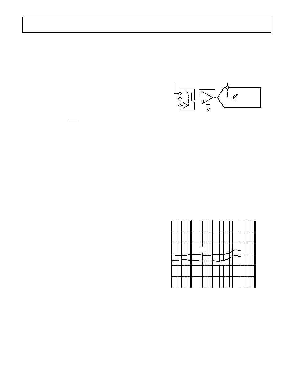
Temperature Sensor
The TEMP pin measures the temperature of the AD7623. To
improve the calibration accuracy over the temperature range,
the output of the TEMP pin is applied to one of the inputs of
the analog switch (such as ADG779), and the ADC itself is used
to measure its own temperature. This configuration is shown
in Figure 28.
05574-028
ADG779
AD8021
CC
ANALOG INPUT
(UNIPOLAR)
AD7623
IN+
TEMPERATURE
SENSOR
TEMP
Figure 28. Use of the Temperature Sensor
POWER SUPPLY
The AD7623 uses three sets of power supply pins: an analog
2.5 V supply AVDD, a digital 2.5 V core supply DVDD, and a
digital input/output interface supply OVDD. The OVDD supply
allows direct interface with any logic working between 2.3 V
and 5.25 V. To reduce the number of supplies needed, the digital
core (DVDD) can be supplied through a simple RC filter from
the analog supply, as shown in Figure 23.
Power Sequencing
The AD7623 is independent of power supply sequencing once
OVDD does not exceed DVDD by more than 0.3 V until
DVDD = 2.3 V during any time; for instance, at power-up or
power-down (see the Absolute Maximum Ratings section).
Additionally, it is very insensitive to power supply variations
over a wide frequency range as shown in Figure 29.
05574-029
FREQUENCY (kHz)
P
S
RR
(dB)
45
75
70
65
60
55
50
1
10
100
1k
10k
EXT REF
INT REF
Figure 29. PSRR vs. Frequency
相关PDF资料 |
PDF描述 |
|---|---|
| AD7703BRZ-REEL | IC ADC 20BIT LC2MOS MONO 20SOIC |
| MS27467T17B26SC | CONN PLUG 26POS STRAIGHT W/SCKT |
| AD7703BR-REEL | IC ADC 20BIT LC2MOS MONO 20-SOIC |
| MS27467T17B26SB | CONN PLUG 26POS STRAIGHT W/SCKT |
| AD8392AAREZ-R7 | IC LINE DRVR ADSL/ADSL 28-TSSOP |
相关代理商/技术参数 |
参数描述 |
|---|---|
| AD7623BD | 制造商:INTERSIL 制造商全称:Intersil Corporation 功能描述:Data Acquisition |
| AD7625 | 制造商:AD 制造商全称:Analog Devices 功能描述:16-Bit, 6MSPS PulSAR Differential ADC |
| AD7625BCPZ | 功能描述:IC ADC 16BIT 6MSPS SAR 32LFCSP RoHS:是 类别:集成电路 (IC) >> 数据采集 - 模数转换器 系列:PulSAR® 其它有关文件:TSA1204 View All Specifications 标准包装:1 系列:- 位数:12 采样率(每秒):20M 数据接口:并联 转换器数目:2 功率耗散(最大):155mW 电压电源:模拟和数字 工作温度:-40°C ~ 85°C 安装类型:表面贴装 封装/外壳:48-TQFP 供应商设备封装:48-TQFP(7x7) 包装:Digi-Reel® 输入数目和类型:4 个单端,单极;2 个差分,单极 产品目录页面:1156 (CN2011-ZH PDF) 其它名称:497-5435-6 |
| AD7625BCPZRL7 | 功能描述:IC ADC 16BIT 6MSPS SAR 32LFCSP RoHS:是 类别:集成电路 (IC) >> 数据采集 - 模数转换器 系列:PulSAR® 标准包装:1 系列:- 位数:14 采样率(每秒):83k 数据接口:串行,并联 转换器数目:1 功率耗散(最大):95mW 电压电源:双 ± 工作温度:0°C ~ 70°C 安装类型:通孔 封装/外壳:28-DIP(0.600",15.24mm) 供应商设备封装:28-PDIP 包装:管件 输入数目和类型:1 个单端,双极 |
| AD7626 | 制造商:AD 制造商全称:Analog Devices 功能描述:16-Bit, 10 MSPS, PulSAR Differential ADC |
发布紧急采购,3分钟左右您将得到回复。