参数资料
| 型号: | AD7626BCPZ |
| 厂商: | Analog Devices Inc |
| 文件页数: | 15/28页 |
| 文件大小: | 0K |
| 描述: | IC ADC 16BIT 10MSPS DIFF 32LFCSP |
| 设计资源: | Single-Ended-to-Differential High Speed Drive Circuit for 16-Bit, 10 MSPS AD7626 ADC (CN0105) |
| 特色产品: | AD7626 PulSAR Differential ADC |
| 标准包装: | 1 |
| 位数: | 16 |
| 采样率(每秒): | 10M |
| 数据接口: | 串行 |
| 转换器数目: | 1 |
| 功率耗散(最大): | 170mW |
| 电压电源: | 模拟和数字 |
| 工作温度: | -40°C ~ 85°C |
| 安装类型: | 表面贴装 |
| 封装/外壳: | 32-VFQFN 裸露焊盘,CSP |
| 供应商设备封装: | 32-LFCSP-VQ(5x5) |
| 包装: | 托盘 |
| 输入数目和类型: | 2 个单端,单极;1 个差分,双极 |
第1页第2页第3页第4页第5页第6页第7页第8页第9页第10页第11页第12页第13页第14页当前第15页第16页第17页第18页第19页第20页第21页第22页第23页第24页第25页第26页第27页第28页
AD7626
Data Sheet
Rev. B | Page 22 of 28
DIGITAL INTERFACE
Conversion Control
All analog-to-digital conversions are controlled by the CNV±
signal. This signal can be applied in the form of a CNV+/CNV
LVDS signal, or it can be applied in the form of a 2.5 V CMOS
logic signal to the CNV+ pin. The conversion is initiated by the
rising edge of the CNV± signal.
After the AD7626 is powered up, the first conversion result
generated is invalid. Subsequent conversion results are valid
provided that the time between conversions does not exceed
the maximum specification for tCYC.
The two methods for acquiring the digital data output of the
AD7626 via the LVDS interface are described in the following
sections.
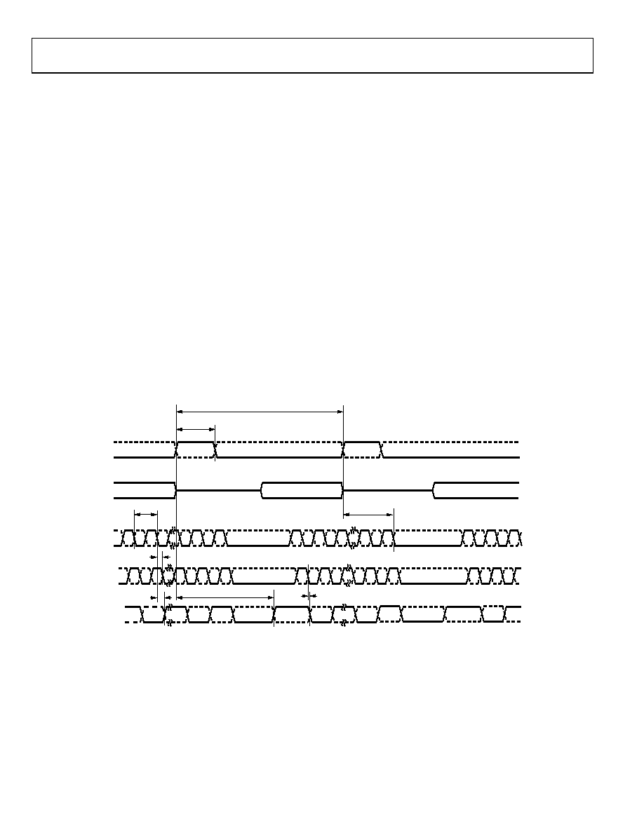
Echoed-Clock Interface Mode
The digital operation of the AD7626 in echoed-clock interface
mode is shown in Figure 41. This interface mode, requiring
only a shift register on the digital host, can be used with many
digital hosts (such as FPGA, shift register, and microprocessor).
It requires three LVDS pairs (D±, CLK±, and DCO±) between
each AD7626 and the digital host.
The clock DCO± is a buffered copy of CLK± and is synchronous
to the data, D±, which is updated on the falling edge of DCO +
(tD). By maintaining good propagation delay matching between
D± and DCO± through the board and the digital host, DCO
can be used to latch D± with good timing margin for the shift
register.
Conversions are initiated by a rising edge CNV± pulse. The
CNV± pulse must be returned low (≤ tCNVH maximum) for
valid operation. After a conversion begins, it continues until
completion. Additional CNV± pulses are ignored during the
conversion phase. After the time, tMSB, elapses, the host should
begin to burst the CLK±. Note that, tMSB, is the maximum time
for the MSB of the new conversion result and should be used as
the gating device for CLK±. The echoed clock, DCO±, and the
data, D, are driven in phase with D± being updated on the
falling edge of DCO+; the host should use the rising edge of
DCO+ to capture D±. The only requirement is that the 16
CLK± pulses finish before the time (tCLKL) elapses of the next
conversion phase or the data is lost. From the tCLKL to tMSB, D±
and DCO± are driven to 0. Set CLK± to idle low between CLK±
bursts.
CLK+
tCYC
16
15
CNV+
116
15
2
123
tCNVH
tCLKL
DCO+
16
15
1
16
15
2
1
23
D+
SAMPLE N
SAMPLE N + 1
D–
D15
N
D14
N
D1
N
CLK–
CNV–
DCO–
D0
N – 1
ACQUISITION
tDCO
tD
tCLK
0
tMSB
D1
N – 1
D15
N + 1
D14
N + 1
D0
N
0
D13
N + 1
tCLKD
0
76
48
-10
3
Figure 41. Echoed-Clock Interface Mode Timing Diagram
相关PDF资料 |
PDF描述 |
|---|---|
| AD7628KN | IC DAC 8BIT DUAL MULTIPLY 20-DIP |
| AD7631BCPZ | IC ADC 18BIT 250KSPS BIP 48LFCSP |
| AD7634BCPZ | IC ADC 18BIT BIPO PROGR 48-LFCSP |
| AD7641BSTZRL | IC ADC 18BIT 2MSPS SAR 48-LQFP |
| AD7643BCPZ | IC ADC 18BIT DIFF W/REF 48LFCSP |
相关代理商/技术参数 |
参数描述 |
|---|---|
| AD7626BCPZ-RL7 | 功能描述:IC ADC 16BIT 10MSPS DIFF 32LFCSP RoHS:是 类别:集成电路 (IC) >> 数据采集 - 模数转换器 系列:- 标准包装:1 系列:- 位数:14 采样率(每秒):83k 数据接口:串行,并联 转换器数目:1 功率耗散(最大):95mW 电压电源:双 ± 工作温度:0°C ~ 70°C 安装类型:通孔 封装/外壳:28-DIP(0.600",15.24mm) 供应商设备封装:28-PDIP 包装:管件 输入数目和类型:1 个单端,双极 |
| AD7628 | 制造商:AD 制造商全称:Analog Devices 功能描述:CMOS Dual 8-Bit Buffered Multiplying DAC |
| AD7628BFN | 制造商:未知厂家 制造商全称:未知厂家 功能描述:8-Bit Digital-to-Analog Converter |
| AD7628BN | 制造商:未知厂家 制造商全称:未知厂家 功能描述:8-Bit Digital-to-Analog Converter |
| AD7628BQ | 制造商:Rochester Electronics LLC 功能描述:- Bulk |
发布紧急采购,3分钟左右您将得到回复。