参数资料
| 型号: | AD7626BCPZ |
| 厂商: | Analog Devices Inc |
| 文件页数: | 17/28页 |
| 文件大小: | 0K |
| 描述: | IC ADC 16BIT 10MSPS DIFF 32LFCSP |
| 设计资源: | Single-Ended-to-Differential High Speed Drive Circuit for 16-Bit, 10 MSPS AD7626 ADC (CN0105) |
| 特色产品: | AD7626 PulSAR Differential ADC |
| 标准包装: | 1 |
| 位数: | 16 |
| 采样率(每秒): | 10M |
| 数据接口: | 串行 |
| 转换器数目: | 1 |
| 功率耗散(最大): | 170mW |
| 电压电源: | 模拟和数字 |
| 工作温度: | -40°C ~ 85°C |
| 安装类型: | 表面贴装 |
| 封装/外壳: | 32-VFQFN 裸露焊盘,CSP |
| 供应商设备封装: | 32-LFCSP-VQ(5x5) |
| 包装: | 托盘 |
| 输入数目和类型: | 2 个单端,单极;1 个差分,双极 |
第1页第2页第3页第4页第5页第6页第7页第8页第9页第10页第11页第12页第13页第14页第15页第16页当前第17页第18页第19页第20页第21页第22页第23页第24页第25页第26页第27页第28页
AD7626
Data Sheet
Rev. B | Page 24 of 28
APPLICATIONS INFORMATION
LAYOUT, DECOUPLING, AND GROUNDING
When laying out the printed circuit board (PCB) for the AD7626,
follow the practices described in this section to obtain the maxi-
mum performance from the converter.
Exposed Paddle
The AD7626 has an exposed paddle on the underside of the
package.
Solder the paddle directly to the PCB.
Connect the paddle to the ground plane of the board using
multiple vias, as shown in Figure 43.
Decouple all supply pins except for Pin 12 (VIO) directly to
the paddle, minimizing the current return path.
Pin 13 and Pin 24 can be connected directly to the paddle.
Use vias to ground at the point where these pins connect to
the paddle.
VDD1 Supply Routing and Decoupling
The VDD1 supply is connected to Pin 1, Pin 19, and Pin 20.
Decouple the supply using a 100 nF capacitor at Pin 1. The user
can connect this supply trace to Pin 19 and Pin 20. Use a series
ferrite bead to connect the VDD1 supply from Pin 1 to Pin 19
and Pin 20. The ferrite bead isolates any high frequency noise or
ringing on the VDD1 supply. Decouple the VDD1 supply to Pin
19 and Pin 20 using a 100 nF capacitor decoupled to ground at
the exposed paddle.
VIO Supply Decoupling
Decouple the VIO supply applied to Pin 12 to ground at Pin 13.
Layout and Decoupling of Pin 25 to Pin 32
Connect the outputs of Pin 25, Pin 26, and Pin 28 together and
decouple them to Pin 27 using a 10 μF capacitor with low ESR
and low ESL.
Reduce the inductance of the path connecting Pin 25, Pin 26,
and Pin 28 by widening the PCB traces connecting these pins.
Take a similar approach in the connections used for the
reference pins of the AD7626. Connect Pin 29, Pin 30, and
Pin 32 together using widened PCB traces to reduce inductance.
In internal or external reference mode, a 4.096 V reference voltage
is output on Pin 29, Pin 30, and Pin 32. Decouple these pins to
Pin 31 using a 10 μF capacitor with low ESR and low ESL.
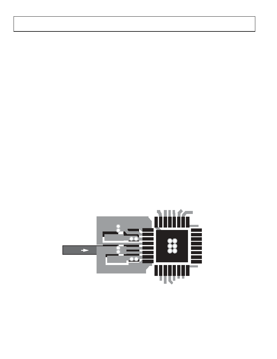
Figure 43 shows an example of the recommended layout for
the underside of the AD7626 device. Note the extended signal
trace connections and the outline of the capacitors decoupling
the signals applied to the REF pins (Pin 29, Pin 30, and Pin 32)
and to the CAP2 pins (Pin 25, Pin 26, and Pin 28).
32
31
30
29
28
27
26
25
PADDLE
1
2
3
4
5
6
7
8
9
10
11
12
13
14
15
16
24 23 22 21 20 19 18 17
4.096V
EXTERNAL REFERENCE
(ADR434 OR ADR444)
07648-
013
Figure 43. PCB Layout and Decoupling Recommendations for Pin 24 to Pin 32
相关PDF资料 |
PDF描述 |
|---|---|
| AD7628KN | IC DAC 8BIT DUAL MULTIPLY 20-DIP |
| AD7631BCPZ | IC ADC 18BIT 250KSPS BIP 48LFCSP |
| AD7634BCPZ | IC ADC 18BIT BIPO PROGR 48-LFCSP |
| AD7641BSTZRL | IC ADC 18BIT 2MSPS SAR 48-LQFP |
| AD7643BCPZ | IC ADC 18BIT DIFF W/REF 48LFCSP |
相关代理商/技术参数 |
参数描述 |
|---|---|
| AD7626BCPZ-RL7 | 功能描述:IC ADC 16BIT 10MSPS DIFF 32LFCSP RoHS:是 类别:集成电路 (IC) >> 数据采集 - 模数转换器 系列:- 标准包装:1 系列:- 位数:14 采样率(每秒):83k 数据接口:串行,并联 转换器数目:1 功率耗散(最大):95mW 电压电源:双 ± 工作温度:0°C ~ 70°C 安装类型:通孔 封装/外壳:28-DIP(0.600",15.24mm) 供应商设备封装:28-PDIP 包装:管件 输入数目和类型:1 个单端,双极 |
| AD7628 | 制造商:AD 制造商全称:Analog Devices 功能描述:CMOS Dual 8-Bit Buffered Multiplying DAC |
| AD7628BFN | 制造商:未知厂家 制造商全称:未知厂家 功能描述:8-Bit Digital-to-Analog Converter |
| AD7628BN | 制造商:未知厂家 制造商全称:未知厂家 功能描述:8-Bit Digital-to-Analog Converter |
| AD7628BQ | 制造商:Rochester Electronics LLC 功能描述:- Bulk |
发布紧急采购,3分钟左右您将得到回复。