参数资料
| 型号: | AD7626BCPZ |
| 厂商: | Analog Devices Inc |
| 文件页数: | 27/28页 |
| 文件大小: | 0K |
| 描述: | IC ADC 16BIT 10MSPS DIFF 32LFCSP |
| 设计资源: | Single-Ended-to-Differential High Speed Drive Circuit for 16-Bit, 10 MSPS AD7626 ADC (CN0105) |
| 特色产品: | AD7626 PulSAR Differential ADC |
| 标准包装: | 1 |
| 位数: | 16 |
| 采样率(每秒): | 10M |
| 数据接口: | 串行 |
| 转换器数目: | 1 |
| 功率耗散(最大): | 170mW |
| 电压电源: | 模拟和数字 |
| 工作温度: | -40°C ~ 85°C |
| 安装类型: | 表面贴装 |
| 封装/外壳: | 32-VFQFN 裸露焊盘,CSP |
| 供应商设备封装: | 32-LFCSP-VQ(5x5) |
| 包装: | 托盘 |
| 输入数目和类型: | 2 个单端,单极;1 个差分,双极 |
第1页第2页第3页第4页第5页第6页第7页第8页第9页第10页第11页第12页第13页第14页第15页第16页第17页第18页第19页第20页第21页第22页第23页第24页第25页第26页当前第27页第28页
AD7626
Data Sheet
Rev. B | Page 8 of 28
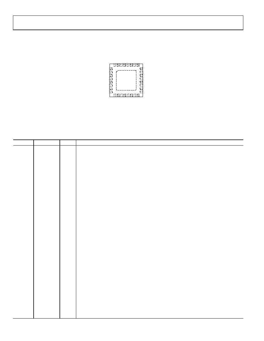
PIN CONFIGURATION AND FUNCTION DESCRIPTIONS
07
648-
0
02
NOTES
1. CONNECT THE EXPOSED PAD TO THE GROUND
PLANE OF THE PCB USING MULTIPLE VIAS.
VDD1
VDD2
CAP1
REFIN
EN0
EN1
VDD2
CNV–
GND
IN+
IN–
VCM
VDD1
VDD2
CLK+
C
N
V
+
D
–
D
+
V
IO
G
N
D
C
O
–
D
C
O
+
C
L
K
–
R
E
F
G
N
D
R
E
F
R
E
F
C
A
P
2
G
N
D
C
A
P
2
C
A
P
2
1
2
3
4
5
6
7
8
24
23
22
21
20
19
18
17
9
10
11
12
13
14
15
16
32
31
30
29
28
27
26
25
AD7626
TOP VIEW
(Not to Scale)
Figure 4. Pin Configuration
Table 6. Pin Function Descriptions
Pin No.
Mnemonic
Type1
Description
1
VDD1
P
Analog 5 V Supply. Decouple the 5 V supply with a 100 nF capacitor.
2
VDD2
P
Analog 2.5 V Supply. Decouple this pin with a 100 nF capacitor. The 2.5 V supply source should
supply this pin first, then be traced to the other VDD2 pins (Pin 7 and Pin 18).
3
CAP1
AO
Connect this pin to a 10 nF capacitor.
4
REFIN
AI/O
Prebuffer Reference Voltage. When using the internal reference, this pin outputs the band gap voltage
and is nominally at 1.2 V. It can be overdriven with an external reference voltage such as the ADR280.
In either internal or external reference mode, a 10 μF capacitor is required. If using an external 4.096 V
reference (connected to REF), this pin is a no connect and does not require any capacitor.
5, 6
EN0, EN1
DI
Enable. Operates from 2.5 V logic. The logic levels of these pins set the operation of the device as
follows:
EN1 = 0, EN0 = 0: power-down mode.
EN1 = 0, EN0 = 1: external 1.2 V reference applied to the REFIN pin required.
EN1 = 1, EN0 = 0: external 4.096 V reference applied to the REF pin required.
EN1 = 1, EN0 = 1: internal reference and internal reference buffer in use.
7
VDD2
P
Digital 2.5 V Supply. Decouple this pin with a 100 nF capacitor.
8, 9
CNV, CNV+
DI
Convert Input. These pins act as the conversion control pin. On the rising edge of these pins, the
analog inputs are sampled and a conversion cycle is initiated. CNV+ works as a CMOS input when
CNV is grounded; otherwise, CNV+ and CNV are differential LVDS inputs.
10, 11
D, D+
DO
LVDS Data Outputs. The conversion data is output serially on these pins.
12
VIO
P
Input/Output Interface Supply. Use a 2.5 V supply and decouple this pin with a 100 nF capacitor.
13
GND
P
Ground. Return path for the 100 nF capacitor connected to Pin 12.
14, 15
DCO, DCO+
DO
LVDS Buffered Clock Outputs. When DCO+ is grounded, the self-clocked interface mode is selected.
In this mode, the 16-bit results on D are preceded by an initial 0 (which is output at the end of the
previous conversion), followed by a 2-bit header (10) to allow synchronization of the data by the
digital host with extra logic. The 1 in this header provides the reference to acquire the subsequent
conversion result correctly. When DCO+ is not grounded, the echoed-clock interface mode is
selected. In this mode, DCO± is a copy of CLK±. The data bits are output on the falling edge of DCO+
and can be captured in the digital host on the next rising edge of DCO+.
16, 17
CLK, CLK+
DI
LVDS Clock Inputs. This clock shifts out the conversion results on the falling edge of CLK+.
18
VDD2
P
Analog 2.5 V Supply. Decouple this pin with a 100 nF capacitor.
19, 20
VDD1
P
Analog 5 V Supply. Isolate these pins from Pin 1 with a ferrite bead and decouple them with a 100 nF
capacitor.
21
VCM
AO
Common-Mode Output. When using any reference scheme, this pin produces one-half the voltage
present on the REF pin, which can be useful for driving the common mode of the input amplifiers.
22
IN
AI
Differential Negative Analog Input. Referenced to and must be driven 180° out of phase with IN+.
23
IN+
AI
Differential Positive Analog Input. Referenced to and must be driven 180° out of phase with IN.
相关PDF资料 |
PDF描述 |
|---|---|
| AD7628KN | IC DAC 8BIT DUAL MULTIPLY 20-DIP |
| AD7631BCPZ | IC ADC 18BIT 250KSPS BIP 48LFCSP |
| AD7634BCPZ | IC ADC 18BIT BIPO PROGR 48-LFCSP |
| AD7641BSTZRL | IC ADC 18BIT 2MSPS SAR 48-LQFP |
| AD7643BCPZ | IC ADC 18BIT DIFF W/REF 48LFCSP |
相关代理商/技术参数 |
参数描述 |
|---|---|
| AD7626BCPZ-RL7 | 功能描述:IC ADC 16BIT 10MSPS DIFF 32LFCSP RoHS:是 类别:集成电路 (IC) >> 数据采集 - 模数转换器 系列:- 标准包装:1 系列:- 位数:14 采样率(每秒):83k 数据接口:串行,并联 转换器数目:1 功率耗散(最大):95mW 电压电源:双 ± 工作温度:0°C ~ 70°C 安装类型:通孔 封装/外壳:28-DIP(0.600",15.24mm) 供应商设备封装:28-PDIP 包装:管件 输入数目和类型:1 个单端,双极 |
| AD7628 | 制造商:AD 制造商全称:Analog Devices 功能描述:CMOS Dual 8-Bit Buffered Multiplying DAC |
| AD7628BFN | 制造商:未知厂家 制造商全称:未知厂家 功能描述:8-Bit Digital-to-Analog Converter |
| AD7628BN | 制造商:未知厂家 制造商全称:未知厂家 功能描述:8-Bit Digital-to-Analog Converter |
| AD7628BQ | 制造商:Rochester Electronics LLC 功能描述:- Bulk |
发布紧急采购,3分钟左右您将得到回复。