参数资料
| 型号: | AD7634BCPZ |
| 厂商: | Analog Devices Inc |
| 文件页数: | 31/32页 |
| 文件大小: | 0K |
| 描述: | IC ADC 18BIT BIPO PROGR 48-LFCSP |
| 标准包装: | 1 |
| 系列: | PulSAR® |
| 位数: | 18 |
| 采样率(每秒): | 670k |
| 数据接口: | 串行,并联 |
| 转换器数目: | 1 |
| 功率耗散(最大): | 225mW |
| 电压电源: | 模拟和数字 |
| 工作温度: | -40°C ~ 85°C |
| 安装类型: | 表面贴装 |
| 封装/外壳: | 48-VFQFN 裸露焊盘,CSP |
| 供应商设备封装: | 48-LFCSP-VQ(7x7) |
| 包装: | 托盘 |
| 输入数目和类型: | 1 个差分,单极;1 个差分,双极 |
第1页第2页第3页第4页第5页第6页第7页第8页第9页第10页第11页第12页第13页第14页第15页第16页第17页第18页第19页第20页第21页第22页第23页第24页第25页第26页第27页第28页第29页第30页当前第31页第32页
AD7634
Data Sheet
Rev. B | Page 8 of 32
PIN CONFIGURATION AND FUNCTION DESCRIPTIONS
P
DBUF
P
DRE
F
RE
F
BUF
IN
TE
M
P
AV
D
IN
+
AG
ND
VEE
VC
C
IN
–
RE
F
G
N
D
RE
F
D6/
E
X
T
/I
NT
D7
/I
NV
S
Y
NC
D8/
INV
S
C
L
K
D
9/
RDC/
S
DI
N
OG
N
D
OV
D
DV
DD
DG
ND
D1
0/
S
D
O
U
T
D
11/
S
DCL
K
D
12
/SYN
C
D1
3/
RDE
RR
O
R
AGND
AVDD
MODE0
MODE1
D0/OB/2C
D1/A0
D3
D4/DIVSCLK[0]
D5/DIVSCLK[1]
IMPULSE
WARP
BIPOLAR
CNVST
PD
RESET
CS
RD
TEN
NOTES
1. FOR THE LEAD FRAME CHIP SCALE PACKAGE (LFCSP), THE EXPOSED PAD
SHOULD BE CONNECTED TO VEE. THIS CONNECTION IS NOT REQUIRED TO
MEET THE ELECTRICAL PERFORMANCES.
BUSY
D17/SCCS
D16/SCCLK
D15/SCIN
D14/HW/SW
48 47 46 45 44 43 42 41 40 39 38 37
35
34
33
30
31
32
36
29
28
27
25
26
2
3
4
7
6
5
1
8
9
10
12
11
13 14 15 16 17 18 19 20 21 22 23 24
PIN 1
AD7634
TOP VIEW
(Not to Scale)
D2/A1
06
406
-004
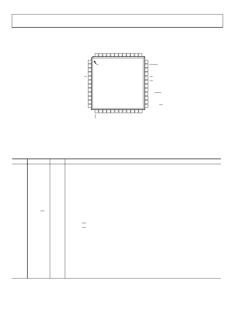
Figure 4. Pin Configuration
Table 6. Pin Function Descriptions
Pin No.
Mnemonic
Type1
Description
1, 42
AGND
P
Analog Power Ground Pins. Ground reference point for all analog I/O. All analog I/O should be refer-
enced to AGND and should be connected to the analog ground plane of the system. In addition, the
AGND, DGND, and OGND voltages should be at the same potential.
2, 44
AVDD
P
Analog Power Pins. Nominally 4.75 V to 5.25 V and decoupled with 10 μF and 100 nF capacitors.
3, 4
MODE[0:1]
DI
Data Input/Output Interface Mode Selection.
Interface Mode
MODE1
MODE0
Description
0
Low
18-bit interface
1
Low
High
16-bit interface
2
High
Low
8-bit (byte) interface
3
High
Serial interface
5
D0/OB/2C
In 18-bit parallel mode, this output is used as Bit 0 of the parallel port data output bus and the data
coding is straight binary. In all other modes, this pin allows the choice of straight binary or twos
complement.
When OB/2C = high, the digital output is straight binary
When OB/2C = low, the MSB is inverted resulting in a twos complement output from its internal shift
register.
6
WARP
Conversion Mode Selection. See the Modes of Operation section for a more detailed description. Used
in conjunction with the IMPULSE input per the following:
Conversion Mode
WARP
IMPULSE
Normal
Low
Impulse
Low
High
Warp
High
Low
Normal
High
7
IMPULSE
Conversion Mode Selection. See the WARP pin description in this table. See the Modes of Operation
section for a more detailed description.
相关PDF资料 |
PDF描述 |
|---|---|
| AD7641BSTZRL | IC ADC 18BIT 2MSPS SAR 48-LQFP |
| AD7643BCPZ | IC ADC 18BIT DIFF W/REF 48LFCSP |
| AD7650ACPZ | IC ADC 16BIT CMOS 5V 48LFCSP |
| AD7651ACPZ | IC ADC 16BIT UNIPOLAR 48LFCSP |
| AD7652ASTZ | IC ADC 16BIT 500KSPS REF 48LQFP |
相关代理商/技术参数 |
参数描述 |
|---|---|
| AD7634BCPZRL | 功能描述:IC ADC 18BIT DIFF BIPO 48-LFCSP RoHS:是 类别:集成电路 (IC) >> 数据采集 - 模数转换器 系列:PulSAR® 标准包装:1 系列:- 位数:14 采样率(每秒):83k 数据接口:串行,并联 转换器数目:1 功率耗散(最大):95mW 电压电源:双 ± 工作温度:0°C ~ 70°C 安装类型:通孔 封装/外壳:28-DIP(0.600",15.24mm) 供应商设备封装:28-PDIP 包装:管件 输入数目和类型:1 个单端,双极 |
| AD7634BSTZ | 功能描述:IC ADC 18BIT DIFF BIPO 48-LQFP RoHS:是 类别:集成电路 (IC) >> 数据采集 - 模数转换器 系列:PulSAR® 标准包装:1 系列:- 位数:14 采样率(每秒):83k 数据接口:串行,并联 转换器数目:1 功率耗散(最大):95mW 电压电源:双 ± 工作温度:0°C ~ 70°C 安装类型:通孔 封装/外壳:28-DIP(0.600",15.24mm) 供应商设备封装:28-PDIP 包装:管件 输入数目和类型:1 个单端,双极 |
| AD7634BSTZRL | 功能描述:IC ADC 18BIT DIFF BIPO 48-LQFP RoHS:是 类别:集成电路 (IC) >> 数据采集 - 模数转换器 系列:PulSAR® 标准包装:1 系列:- 位数:14 采样率(每秒):83k 数据接口:串行,并联 转换器数目:1 功率耗散(最大):95mW 电压电源:双 ± 工作温度:0°C ~ 70°C 安装类型:通孔 封装/外壳:28-DIP(0.600",15.24mm) 供应商设备封装:28-PDIP 包装:管件 输入数目和类型:1 个单端,双极 |
| AD7641 | 制造商:AD 制造商全称:Analog Devices 功能描述:16-Bit, 750 kSPS, Unipolar/Bipolar Programmable Input PulSAR ADC |
| AD7641ACP | 制造商:Analog Devices 功能描述:ADC SGL SAR 2MSPS 18BIT PARALLEL/SERL 48LFCSP - Trays |
发布紧急采购,3分钟左右您将得到回复。