- 您现在的位置:买卖IC网 > PDF目录10167 > AD7654ASTZRL (Analog Devices Inc)IC ADC 16BIT DUAL 2CH 48LQFP PDF资料下载
参数资料
| 型号: | AD7654ASTZRL |
| 厂商: | Analog Devices Inc |
| 文件页数: | 11/28页 |
| 文件大小: | 0K |
| 描述: | IC ADC 16BIT DUAL 2CH 48LQFP |
| 标准包装: | 2,000 |
| 系列: | PulSAR® |
| 位数: | 16 |
| 采样率(每秒): | 500k |
| 数据接口: | 串行,并联 |
| 转换器数目: | 1 |
| 功率耗散(最大): | 135mW |
| 电压电源: | 模拟和数字 |
| 工作温度: | -40°C ~ 85°C |
| 安装类型: | 表面贴装 |
| 封装/外壳: | 48-LQFP |
| 供应商设备封装: | 48-LQFP(7x7) |
| 包装: | 带卷 (TR) |
| 输入数目和类型: | 2 个差分,单极 |
| 配用: | EVAL-AD7654CBZ-ND - BOARD EVALUATION FOR AD7654 |
第1页第2页第3页第4页第5页第6页第7页第8页第9页第10页当前第11页第12页第13页第14页第15页第16页第17页第18页第19页第20页第21页第22页第23页第24页第25页第26页第27页第28页
AD7654
Rev. B | Page 19 of 28
t1
t3
t4
t17
BUSY
DATA
BUS
t16
NEW A
OR B
PREVIOUS CHANNEL A
OR B
PREVIOUS CHANNEL B
OR NEW A
t10
CS = RD = 0
EOC
CNVST
03
05
7-
02
4
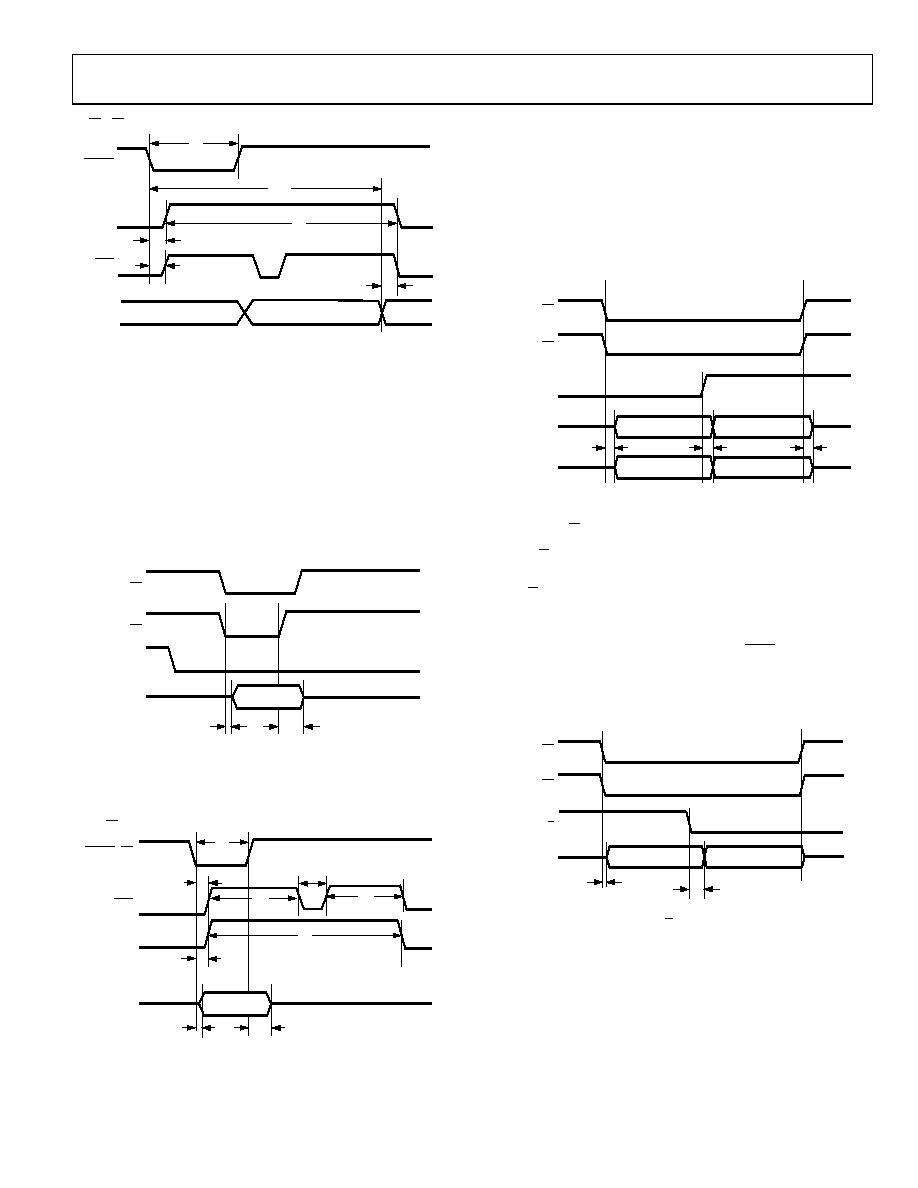
Figure 24. Master Parallel Data Timing for Continuous Read
Slave Parallel Interface
In slave parallel reading mode, the data can be read either after
each conversion, which is during the next acquisition phase or
during the other channel’s conversion, or during the following
When the data is read during the conversion, however, it is
recommended that it is read only during the first half of the
conversion phase. This avoids any potential feedthrough
between voltage transients on the digital interface and the most
critical analog conversion circuitry.
DATA BUS
t18
t19
BUSY
CURRENT
CONVERSION
CS
RD
03
05
7-
02
5
Figure 25. Slave Parallel Data Timing for a Read After Conversion
PREVIOUS
CONVERSION
t1
t3
t18
t19
t4
BUSY
DATA BUS
t13
t11
t12
t10
CS =0
EOC
CNVST, RD
03
05
7-
02
6
Figure 26. Slave Parallel Data Timing for a Read During Conversion
8-Bit Interface (Master or Slave)
The BYTESWAP pin allows a glueless interface to an 8-bit bus.
As shown in Figure 27, the LSB byte is output on D[7:0] and the
MSB is output on D[15:8] when BYTESWAP is low. When
BYTESWAP is high, the LSB and MSB bytes are swapped, the
LSB is output on D[15:8], and the MSB is output on D[7:0]. By
connecting BYTESWAP to an address line, the 16-bit data can
be read in two bytes on either D[15:8] or D[7:0].
BYTESWAP
PINS D[15:8]
PINS D[7:0]
HI-Z
HIGH BYTE
LOW BYTE
HIGH BYTE
HI-Z
t18
t19
CS
RD
03
05
7-
02
7
Figure 27. 8-Bit Parallel Interface
Channel A/B Output
The A/B input controls which channel’s conversion results
(INAx or INBx) are output on the data bus. The functionality
of A/B is detailed in Figure 28. When high, the data from
Channel A is available on the data bus. When low, the data from
Channel B is available on the bus. Note that Channel A can be
read immediately after conversion is done (EOC), while
Channel B is still in its converting phase. However, in any of the
serial reading modes, Channel A data is updated only after
Channel B is converted.
t18
t20
CS
DATA BUS
RD
HI-Z
A/B
HI-Z
CHANNEL A
CHANNEL B
03
05
7-
0
28
Figure 28. A/B Channel Reading
相关PDF资料 |
PDF描述 |
|---|---|
| VI-2NZ-MV-F2 | CONVERTER MOD DC/DC 2V 60W |
| IDT72V285L15TFI | IC FIFO SS 65536X18 15NS 64STQFP |
| VI-B7M-MY | CONVERTER MOD DC/DC 10V 50W |
| ADM202EARN | IC TXRX RS-232 5V 15KV 16SOIC |
| IDT72V3690L15PF | IC FIFO SS 32768X36 15NS 128TQFP |
相关代理商/技术参数 |
参数描述 |
|---|---|
| AD7655 | 制造商:AD 制造商全称:Analog Devices 功能描述:14-Bit, 1 MSPS, Differential, Programmable Input PulSAR ADC |
| AD7655ACP | 制造商:Analog Devices 功能描述:ADC Single SAR 1Msps 16-bit Parallel/Serial 48-Pin LFCSP EP 制造商:Rochester Electronics LLC 功能描述:LOW COST 4-CHANNEL 1 MSPS 16-BIT ADC - Bulk 制造商:Analog Devices 功能描述:IC 16BIT ADC SMD 7655 LFSCP-48 |
| AD7655ACPRL | 制造商:Analog Devices 功能描述:ADC Single SAR 1Msps 16-bit Parallel/Serial 48-Pin LFCSP EP T/R |
| AD7655ACPZ | 功能描述:IC ADC 16BIT 4CH 48-LFCSP RoHS:是 类别:集成电路 (IC) >> 数据采集 - 模数转换器 系列:PulSAR® 标准包装:1 系列:microPOWER™ 位数:8 采样率(每秒):1M 数据接口:串行,SPI? 转换器数目:1 功率耗散(最大):- 电压电源:模拟和数字 工作温度:-40°C ~ 125°C 安装类型:表面贴装 封装/外壳:24-VFQFN 裸露焊盘 供应商设备封装:24-VQFN 裸露焊盘(4x4) 包装:Digi-Reel® 输入数目和类型:8 个单端,单极 产品目录页面:892 (CN2011-ZH PDF) 其它名称:296-25851-6 |
| AD7655ACPZRL | 功能描述:IC ADC 16BIT 4CHAN 48LFCSP RoHS:是 类别:集成电路 (IC) >> 数据采集 - 模数转换器 系列:PulSAR® 标准包装:1,000 系列:- 位数:12 采样率(每秒):300k 数据接口:并联 转换器数目:1 功率耗散(最大):75mW 电压电源:单电源 工作温度:0°C ~ 70°C 安装类型:表面贴装 封装/外壳:24-SOIC(0.295",7.50mm 宽) 供应商设备封装:24-SOIC 包装:带卷 (TR) 输入数目和类型:1 个单端,单极;1 个单端,双极 |
发布紧急采购,3分钟左右您将得到回复。