- 您现在的位置:买卖IC网 > PDF目录10167 > AD7654ASTZRL (Analog Devices Inc)IC ADC 16BIT DUAL 2CH 48LQFP PDF资料下载
参数资料
| 型号: | AD7654ASTZRL |
| 厂商: | Analog Devices Inc |
| 文件页数: | 15/28页 |
| 文件大小: | 0K |
| 描述: | IC ADC 16BIT DUAL 2CH 48LQFP |
| 标准包装: | 2,000 |
| 系列: | PulSAR® |
| 位数: | 16 |
| 采样率(每秒): | 500k |
| 数据接口: | 串行,并联 |
| 转换器数目: | 1 |
| 功率耗散(最大): | 135mW |
| 电压电源: | 模拟和数字 |
| 工作温度: | -40°C ~ 85°C |
| 安装类型: | 表面贴装 |
| 封装/外壳: | 48-LQFP |
| 供应商设备封装: | 48-LQFP(7x7) |
| 包装: | 带卷 (TR) |
| 输入数目和类型: | 2 个差分,单极 |
| 配用: | EVAL-AD7654CBZ-ND - BOARD EVALUATION FOR AD7654 |
第1页第2页第3页第4页第5页第6页第7页第8页第9页第10页第11页第12页第13页第14页当前第15页第16页第17页第18页第19页第20页第21页第22页第23页第24页第25页第26页第27页第28页
AD7654
Rev. B | Page 22 of 28
SLAVE SERIAL INTERFACE
External Clock
The AD7654 is configured to accept an externally supplied
serial data clock on the SCLK pin when the EXT/INT pin is
held high. In this mode, several methods can be used to read
the data. The external serial clock is gated by CS. When both CS
and RD are low, the data can be read after each conversion or
during the following conversion. The external clock can be
either a continuous or discontinuous clock. A discontinuous
clock can be either normally high or normally low when
diagrams of these methods.
While the AD7654 is performing a bit decision, it is important
that voltage transients not occur on digital input/output pins or
degradation of the conversion result could occur. This is
particularly important during the second half of the conversion
phase of each channel because the AD7654 provides error
correction circuitry that can correct for an improper bit
decision made during the first half of the conversion phase. For
this reason, it is recommended that when an external clock is
provided, it is a discontinuous clock that toggles only when
BUSY is low or, more importantly, that it does not transition
during the latter half of EOC high.
External Discontinuous Clock Data Read After Convert
Although the maximum throughput cannot be achieved in this
mode, it is the most recommended of the serial slave modes.
Figure 32 shows the detailed timing diagrams of this method.
After a conversion is complete, indicated by BUSY returning
low, the conversion results can be read while both CS and RD
are low. Data is shifted out from both channels MSB first, with
32 clock pulses and is valid on both rising and falling edges of
the clock.
One advantage of this method is that conversion performance is
not degraded because there are no voltage transients on the
digital interface during the conversion process. Another
advantage is the ability to read the data at any speed up to 40
MHz, which accommodates both a slow digital host interface
and the fastest serial reading.
Finally, in this mode only, the AD7654 provides a daisy-chain
feature using the RDC/SDIN (serial data in) input pin for
cascading multiple converters together. This feature is useful for
reducing component count and wiring connections when it is
desired, as in isolated multiconverter applications.
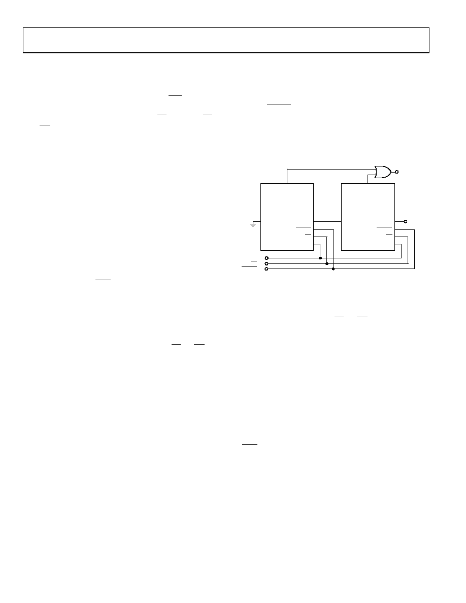
An example of the concatenation of two devices is shown in
Figure 31. Simultaneous sampling is possible by using a
common CNVST signal. Note that the RDC/SDIN input is
latched on the edge of SCLK opposite the one used to shift out
the data on SDOUT. Therefore, the MSB of the upstream
converter follows the LSB of the downstream converter on the
next SCLK cycle. The SDIN input should be tied either high or
low on the most upstream converter in the chain.
BUSY
AD7654
#2 (UPSTREAM)
AD7654
#1 (DOWNSTREAM)
RDC/SDIN
SDOUT
CNVST
CS
SCLK
RDC/SDIN
SDOUT
CNVST
CS
SCLK
DATA
OUT
SCLK IN
CS IN
CNVST IN
BUSY
OUT
03
05
7-
0
31
Figure 31. Two AD7654s in a Daisy-Chain Configuration
External Clock Data Read Previous During Convert
Figure 33 shows the detailed timing diagrams of this method.
During a conversion, while both CS and RD are low, the result
of the previous conversion can be read. The data is shifted out
MSB first with 32 clock pulses and is valid on both the rising
and falling edges of the clock. The 32 bits have to be read before
the current conversion is completed; otherwise, RDERROR is
pulsed high and can be used to interrupt the host interface to
prevent incomplete data reading. There is no daisy-chain
feature in this mode, and RDC/SDIN input should always be
tied either high or low.
To reduce performance degradation due to digital activity, a
fast discontinuous clock (at least 32 MHz in impulse mode and
40 MHz in normal mode) is recommended to ensure that all of
the bits are read during the first half of each conversion phase
(EOC high, t11, t12).
It is also possible to begin to read data after conversion and
continue to read the last bits after a new conversion has been
initiated. This allows the use of a slower clock speed like
26 MHz in impulse mode and 30 MHz in normal mode.
相关PDF资料 |
PDF描述 |
|---|---|
| VI-2NZ-MV-F2 | CONVERTER MOD DC/DC 2V 60W |
| IDT72V285L15TFI | IC FIFO SS 65536X18 15NS 64STQFP |
| VI-B7M-MY | CONVERTER MOD DC/DC 10V 50W |
| ADM202EARN | IC TXRX RS-232 5V 15KV 16SOIC |
| IDT72V3690L15PF | IC FIFO SS 32768X36 15NS 128TQFP |
相关代理商/技术参数 |
参数描述 |
|---|---|
| AD7655 | 制造商:AD 制造商全称:Analog Devices 功能描述:14-Bit, 1 MSPS, Differential, Programmable Input PulSAR ADC |
| AD7655ACP | 制造商:Analog Devices 功能描述:ADC Single SAR 1Msps 16-bit Parallel/Serial 48-Pin LFCSP EP 制造商:Rochester Electronics LLC 功能描述:LOW COST 4-CHANNEL 1 MSPS 16-BIT ADC - Bulk 制造商:Analog Devices 功能描述:IC 16BIT ADC SMD 7655 LFSCP-48 |
| AD7655ACPRL | 制造商:Analog Devices 功能描述:ADC Single SAR 1Msps 16-bit Parallel/Serial 48-Pin LFCSP EP T/R |
| AD7655ACPZ | 功能描述:IC ADC 16BIT 4CH 48-LFCSP RoHS:是 类别:集成电路 (IC) >> 数据采集 - 模数转换器 系列:PulSAR® 标准包装:1 系列:microPOWER™ 位数:8 采样率(每秒):1M 数据接口:串行,SPI? 转换器数目:1 功率耗散(最大):- 电压电源:模拟和数字 工作温度:-40°C ~ 125°C 安装类型:表面贴装 封装/外壳:24-VFQFN 裸露焊盘 供应商设备封装:24-VQFN 裸露焊盘(4x4) 包装:Digi-Reel® 输入数目和类型:8 个单端,单极 产品目录页面:892 (CN2011-ZH PDF) 其它名称:296-25851-6 |
| AD7655ACPZRL | 功能描述:IC ADC 16BIT 4CHAN 48LFCSP RoHS:是 类别:集成电路 (IC) >> 数据采集 - 模数转换器 系列:PulSAR® 标准包装:1,000 系列:- 位数:12 采样率(每秒):300k 数据接口:并联 转换器数目:1 功率耗散(最大):75mW 电压电源:单电源 工作温度:0°C ~ 70°C 安装类型:表面贴装 封装/外壳:24-SOIC(0.295",7.50mm 宽) 供应商设备封装:24-SOIC 包装:带卷 (TR) 输入数目和类型:1 个单端,单极;1 个单端,双极 |
发布紧急采购,3分钟左右您将得到回复。