- 您现在的位置:买卖IC网 > PDF目录10532 > AD7656YSTZ-1 (Analog Devices Inc)IC ADC 16BIT 6CH 250KSPS 64LQFP PDF资料下载
参数资料
| 型号: | AD7656YSTZ-1 |
| 厂商: | Analog Devices Inc |
| 文件页数: | 17/32页 |
| 文件大小: | 0K |
| 描述: | IC ADC 16BIT 6CH 250KSPS 64LQFP |
| 标准包装: | 1 |
| 位数: | 16 |
| 采样率(每秒): | 250k |
| 数据接口: | 串行,并联 |
| 转换器数目: | 6 |
| 功率耗散(最大): | 143mW |
| 电压电源: | 模拟和数字,双 ± |
| 工作温度: | -40°C ~ 125°C |
| 安装类型: | 表面贴装 |
| 封装/外壳: | 64-LQFP |
| 供应商设备封装: | 64-LQFP(10x10) |
| 包装: | 托盘 |
| 输入数目和类型: | 6 个单端,双极 |
| 配用: | EVAL-AD7656-1EDZ-ND - BOARD EVAL CONTROL AD7656-1 EVAL-AD7656-1CBZ-ND - BOARD EVAL FOR AD7656-1 EVAL-AD7656CBZ-ND - BOARD EVAL FOR AD7656 |
第1页第2页第3页第4页第5页第6页第7页第8页第9页第10页第11页第12页第13页第14页第15页第16页当前第17页第18页第19页第20页第21页第22页第23页第24页第25页第26页第27页第28页第29页第30页第31页第32页
AD7656-1/AD7657-1/AD7658-1
Data Sheet
Rev. D | Page 24 of 32
SOFTWARE SELECTION OF ADCS
The H/S SEL pin determines the source of the combination of ADCs
that are to be simultaneously sampled. When the H/S SEL pin
is logic low, the combination of channels to be simultaneously
sampled is determined by the CONVST A, CONVST B, and
CONVST C pins. When the H/S SEL pin is logic high, the
combination of channels selected for simultaneous sampling
is determined by the contents of the DB15 to DB13 control
registers. In this mode, a write to the control register is necessary.
The control register is an 8-bit write-only register. Data is written
to this register using the CS and WR pins and the DB[15:8] data
pins (see Figure 31). The control register is detailed in Table 10
and Table 11. To select an ADC pair to be simultaneously sampled,
set the corresponding data line high during the write operation.
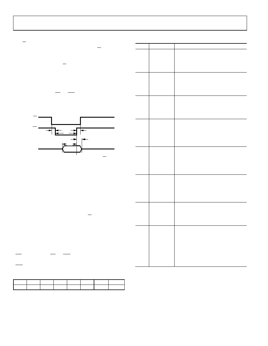
DATA
DB15 TO DB8
CS
t13
t15
t14
t11
t12
WR
07017-
029
Figure 31. Parallel Interface—Write Cycle for Word Mode (W/B = 0)
The AD7656-1/AD7657-1/AD7658-1 control register allows
individual ranges to be programmed on each ADC pair. DB12
to DB10 in the control register are used to program the range
on each ADC pair.
After a reset occurs on the AD7656-1/AD7657-1/AD7658-1,
the control register contains all 0s.
The CONVST A signal is used to initiate a simultaneous
conversion on the combination of channels selected via the
control register. The CONVST B and CONVST C signals can be
tied low when operating in software mode (H/S SEL = 1). The
number of read pulses required depends on the number of
ADCs selected in the control register and on whether the
devices are operating in word or byte mode. The conversion
results are output in ascending order.
During the write operation, Data Bus Bit DB15 to Data Bus Bit DB8
are bidirectional and become inputs to the control register when
RD is logic high and CS and WR are logic low. The logic state
on DB15 through DB8 is latched into the control register when
WR goes logic high.
Table 10. Control Register Bit Map1
DB15
DB14
DB13
DB12
DB11
DB10
DB9
DB8
VC
VB
VA
RNGC
RNGB
RNGA
REFEN
REFBUF
1
Default all 0s.
Table 11. Control Register Bit Function Descriptions
Bit
Mnemonic
Description
DB15
VC
This bit is used to select the V5 and V6
analog inputs for the next conversion.
When this bit is set to 1, V5 and V6 are
simultaneously converted on the next
CONVST A rising edge.
DB14
VB
This bit is used to select the V3 and V4
analog inputs for the next conversion.
When this bit is set to 1, V3 and V4 are
simultaneously converted on the next
CONVST A rising edge.
DB13
VA
This bit is used to select the V1 and V2
analog inputs for the next conversion.
When this bit is set to 1, V1 and V2 are
simultaneously converted on the next
CONVST A rising edge.
DB12
RNGC
This bit is used to select the analog input
range for the V5 and V6 analog inputs.
When this bit is set to 1, the ±2 × VREF range
is selected for the next conversion. When
this bit is set to 0, the ±4 × VREF range is
selected for the next conversion.
DB11
RNGB
This bit is used to select the analog input
range for the V3 and V4 analog inputs.
When this bit is set to 1, the ±2 × VREF range
is selected for the next conversion. When
this bit is set to 0, the ±4 × VREF range is
selected for the next conversion.
DB10
RNGA
This bit is used to select the analog input
range for the V1 and V2 analog inputs.
When this bit is set to 1, the ±2 × VREF range
is selected for the next conversion. When
this bit is set to 0, the ±4 × VREF range is
selected for the next conversion.
DB9
REFEN
This bit is used to select the internal
reference or an external reference. When
this bit is set to 0, the external reference
mode is selected. When this bit is set to 1,
the internal reference is selected.
DB8
REFBUF
This bit is used to select between using the
internal reference buffers and choosing
to bypass these reference buffers. When
this bit is set to 0, the internal reference
buffers are enabled and decoupling is
required on the REFCAPx pins. When this
bit is set to 1, the internal reference buffers
are disabled and a buffered reference
should be applied to the REFCAPx pins.
相关PDF资料 |
PDF描述 |
|---|---|
| VE-J4Z-MY-F2 | CONVERTER MOD DC/DC 2V 20W |
| VE-J4Y-MY-F1 | CONVERTER MOD DC/DC 3.3V 33W |
| AD7656YSTZ | IC ADC 16BIT 6CH 250KSPS 64LQFP |
| VE-J4Y-MW-F4 | CONVERTER MOD DC/DC 3.3V 66W |
| VI-B53-MW | CONVERTER MOD DC/DC 24V 100W |
相关代理商/技术参数 |
参数描述 |
|---|---|
| AD7656YSTZ-1-RL | 功能描述:IC ADC 16BIT 6CH 250KSPS 64LQFP RoHS:是 类别:集成电路 (IC) >> 数据采集 - 模数转换器 系列:- 标准包装:1,000 系列:- 位数:12 采样率(每秒):300k 数据接口:并联 转换器数目:1 功率耗散(最大):75mW 电压电源:单电源 工作温度:0°C ~ 70°C 安装类型:表面贴装 封装/外壳:24-SOIC(0.295",7.50mm 宽) 供应商设备封装:24-SOIC 包装:带卷 (TR) 输入数目和类型:1 个单端,单极;1 个单端,双极 |
| AD7656YSTZ-REEL | 功能描述:IC ADC 16BIT 6CH 250KSPS 64LQFP RoHS:是 类别:集成电路 (IC) >> 数据采集 - 模数转换器 系列:- 标准包装:1,000 系列:- 位数:12 采样率(每秒):300k 数据接口:并联 转换器数目:1 功率耗散(最大):75mW 电压电源:单电源 工作温度:0°C ~ 70°C 安装类型:表面贴装 封装/外壳:24-SOIC(0.295",7.50mm 宽) 供应商设备封装:24-SOIC 包装:带卷 (TR) 输入数目和类型:1 个单端,单极;1 个单端,双极 |
| AD7657 | 制造商:AD 制造商全称:Analog Devices 功能描述:250 kSPS, 6-Channel,Simultaneous Sampling, Bipolar 12/14/16-Bit ADC |
| AD7657-1 | 制造商:AD 制造商全称:Analog Devices 功能描述:250 kSPS, 6-Channel, Simultaneous Sampling, Bipolar, 16-/14-/12-Bit ADC |
| AD7657BSTZ | 功能描述:IC ADC 14BIT 6CH 250KSPS 64-LQFP RoHS:是 类别:集成电路 (IC) >> 数据采集 - 模数转换器 系列:- 标准包装:1 系列:microPOWER™ 位数:8 采样率(每秒):1M 数据接口:串行,SPI? 转换器数目:1 功率耗散(最大):- 电压电源:模拟和数字 工作温度:-40°C ~ 125°C 安装类型:表面贴装 封装/外壳:24-VFQFN 裸露焊盘 供应商设备封装:24-VQFN 裸露焊盘(4x4) 包装:Digi-Reel® 输入数目和类型:8 个单端,单极 产品目录页面:892 (CN2011-ZH PDF) 其它名称:296-25851-6 |
发布紧急采购,3分钟左右您将得到回复。