- 您现在的位置:买卖IC网 > PDF目录10532 > AD7656YSTZ-1 (Analog Devices Inc)IC ADC 16BIT 6CH 250KSPS 64LQFP PDF资料下载
参数资料
| 型号: | AD7656YSTZ-1 |
| 厂商: | Analog Devices Inc |
| 文件页数: | 3/32页 |
| 文件大小: | 0K |
| 描述: | IC ADC 16BIT 6CH 250KSPS 64LQFP |
| 标准包装: | 1 |
| 位数: | 16 |
| 采样率(每秒): | 250k |
| 数据接口: | 串行,并联 |
| 转换器数目: | 6 |
| 功率耗散(最大): | 143mW |
| 电压电源: | 模拟和数字,双 ± |
| 工作温度: | -40°C ~ 125°C |
| 安装类型: | 表面贴装 |
| 封装/外壳: | 64-LQFP |
| 供应商设备封装: | 64-LQFP(10x10) |
| 包装: | 托盘 |
| 输入数目和类型: | 6 个单端,双极 |
| 配用: | EVAL-AD7656-1EDZ-ND - BOARD EVAL CONTROL AD7656-1 EVAL-AD7656-1CBZ-ND - BOARD EVAL FOR AD7656-1 EVAL-AD7656CBZ-ND - BOARD EVAL FOR AD7656 |
第1页第2页当前第3页第4页第5页第6页第7页第8页第9页第10页第11页第12页第13页第14页第15页第16页第17页第18页第19页第20页第21页第22页第23页第24页第25页第26页第27页第28页第29页第30页第31页第32页
Data Sheet
AD7656-1/AD7657-1/AD7658-1
Rev. D | Page 11 of 32
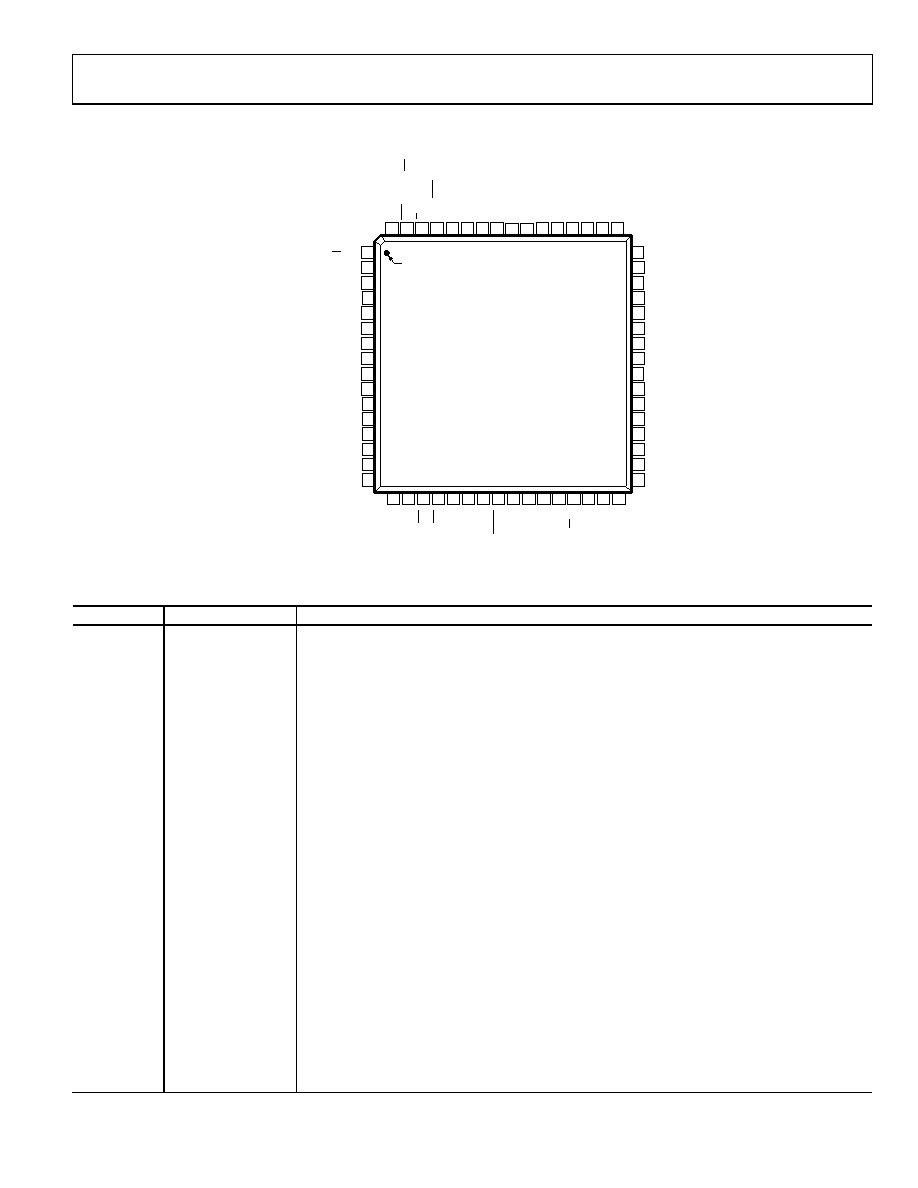
PIN CONFIGURATION AND FUNCTION DESCRIPTIONS
64
DB15
63
W
R/
RE
F
E
N/
DI
S
62
H
/S
SE
L
61
SER
/P
AR
S
E
L
60
A
V
CC
59
AG
ND
58
RE
F
CAP
C
57
AG
ND
56
RE
F
CAP
B
55
AG
ND
54
RE
F
CA
P
A
53
AG
ND
52
AG
ND
51
R
E
FIN
/R
E
FOU
T
50
A
V
CC
49
AG
ND
47
AVCC
46
AVCC
45
V5
42
V4
43
AGND
44
AGND
48
V6
41
AVCC
40
AVCC
39
V3
37
AGND
36
V2
35
AVCC
34
AVCC
33
V1
38
AGND
2
DB13
3
DB12
4
DB11
7
DB8/DOUT A
6
DB9/DOUT B
5
DB10/DOUT C
1
DB14/REFBUFEN/DIS
8
DGND
9
VDRIVE
10
DB7/HBEN/DCEN
12
DB5/DCIN A
13
DB4/DCIN B
14
DB3/DCIN C
15
DB2/SEL C
16
DB1/SEL B
11
DB6/SCLK
17
DB0/
S
E
L
A
18
BUS
Y
19
CS
20
RD
21
CO
NV
S
T
C
22
CO
NV
S
T
B
23
CO
NV
S
T
A
24
ST
B
Y
25
DG
ND
26
DV
CC
27
RANG
E
28
R
ESET
29
W/B
30
V
SS
31
V
DD
32
AG
ND
PIN 1
AD7656-1/AD7657-1/AD7658-1
TOP VIEW
(Not to Scale)
07017-
003
Figure 3. Pin Configuration
Table 7. Pin Function Descriptions
Pin No.
Mnemonic
Description
54, 56, 58
REFCAPA, REFCAPB,
REFCAPC
Reference Capacitor A, Reference Capacitor B, and Reference Capacitor C. Decoupling capacitors are
connected to these pins to decouple the reference buffer for each ADC pair. Decouple each REFCAP pin
to AGND using a 1 F capacitor.
33, 36, 39,
42, 45, 48
V1 to V6
Analog Input 1 to Analog Input 6. These pins are single-ended analog inputs. In hardware mode,
the analog input range of these channels is determined by the RANGE pin. In software mode, it is
determined by the RNGC to RNGA bits of the control register (see Table 11).
32, 37, 38, 43,
44, 49, 52, 53,
55, 57, 59
AGND
Analog Ground. This pin is the ground reference point for all analog circuitry on the AD7656-1/
AD7657-1/AD7658-1. Refer all analog input signals and external reference signals to this pin.
Connect all AGND pins to the AGND plane of the system. The AGND and DGND voltages should
ideally be at the same potential and must not be more than 0.3 V apart, even on a transient basis.
26
DVCC
Digital Power, 4.75 V to 5.25 V. The DVCC and AVCC voltages should ideally be at the same potential
and must not be more than 0.3 V apart, even on a transient basis. Decouple this supply to DGND by
placing a 1 F decoupling capacitor on the DVCC pin.
9
VDRIVE
Logic Power Supply Input. The voltage supplied at this pin determines the operating voltage of the
interface. This pin is nominally at the same supply as the supply of the host interface.
8, 25
DGND
Digital Ground. This is the ground reference point for all digital circuitry on the AD7656-1/AD7657-1/
AD7658-1. Connect both DGND pins to the DGND plane of a system. The DGND and AGND voltages
should ideally be at the same potential and must not be more than 0.3 V apart, even on a transient
basis.
34, 35, 40,
41, 46, 47,
50, 60
AVCC
Analog Supply Voltage, 4.75 V to 5.25 V. This is the supply voltage for the ADC cores. The AVCC and
DVCC voltages should ideally be at the same potential and must not be more than 0.3 V apart, even
on a transient basis.
21, 22, 23
CONVST C,
CONVST B, CONVST A
Conversion Start Input A, Conversion Start Input B, and Conversion Start Input C. These logic inputs
are used to initiate conversions on the ADC pairs. CONVST A is used to initiate simultaneous conversions
on V1 and V2. CONVST B is used to initiate simultaneous conversions on V3 and V4. CONVST C is
used to initiate simultaneous conversions on V5 and V6. When one of these pins switches from low
to high, the track-and-hold switch on the selected ADC pair switches from track to hold, and the
conversion is initiated. These inputs can also be used to place the ADC pairs into partial power-
down mode.
相关PDF资料 |
PDF描述 |
|---|---|
| VE-J4Z-MY-F2 | CONVERTER MOD DC/DC 2V 20W |
| VE-J4Y-MY-F1 | CONVERTER MOD DC/DC 3.3V 33W |
| AD7656YSTZ | IC ADC 16BIT 6CH 250KSPS 64LQFP |
| VE-J4Y-MW-F4 | CONVERTER MOD DC/DC 3.3V 66W |
| VI-B53-MW | CONVERTER MOD DC/DC 24V 100W |
相关代理商/技术参数 |
参数描述 |
|---|---|
| AD7656YSTZ-1-RL | 功能描述:IC ADC 16BIT 6CH 250KSPS 64LQFP RoHS:是 类别:集成电路 (IC) >> 数据采集 - 模数转换器 系列:- 标准包装:1,000 系列:- 位数:12 采样率(每秒):300k 数据接口:并联 转换器数目:1 功率耗散(最大):75mW 电压电源:单电源 工作温度:0°C ~ 70°C 安装类型:表面贴装 封装/外壳:24-SOIC(0.295",7.50mm 宽) 供应商设备封装:24-SOIC 包装:带卷 (TR) 输入数目和类型:1 个单端,单极;1 个单端,双极 |
| AD7656YSTZ-REEL | 功能描述:IC ADC 16BIT 6CH 250KSPS 64LQFP RoHS:是 类别:集成电路 (IC) >> 数据采集 - 模数转换器 系列:- 标准包装:1,000 系列:- 位数:12 采样率(每秒):300k 数据接口:并联 转换器数目:1 功率耗散(最大):75mW 电压电源:单电源 工作温度:0°C ~ 70°C 安装类型:表面贴装 封装/外壳:24-SOIC(0.295",7.50mm 宽) 供应商设备封装:24-SOIC 包装:带卷 (TR) 输入数目和类型:1 个单端,单极;1 个单端,双极 |
| AD7657 | 制造商:AD 制造商全称:Analog Devices 功能描述:250 kSPS, 6-Channel,Simultaneous Sampling, Bipolar 12/14/16-Bit ADC |
| AD7657-1 | 制造商:AD 制造商全称:Analog Devices 功能描述:250 kSPS, 6-Channel, Simultaneous Sampling, Bipolar, 16-/14-/12-Bit ADC |
| AD7657BSTZ | 功能描述:IC ADC 14BIT 6CH 250KSPS 64-LQFP RoHS:是 类别:集成电路 (IC) >> 数据采集 - 模数转换器 系列:- 标准包装:1 系列:microPOWER™ 位数:8 采样率(每秒):1M 数据接口:串行,SPI? 转换器数目:1 功率耗散(最大):- 电压电源:模拟和数字 工作温度:-40°C ~ 125°C 安装类型:表面贴装 封装/外壳:24-VFQFN 裸露焊盘 供应商设备封装:24-VQFN 裸露焊盘(4x4) 包装:Digi-Reel® 输入数目和类型:8 个单端,单极 产品目录页面:892 (CN2011-ZH PDF) 其它名称:296-25851-6 |
发布紧急采购,3分钟左右您将得到回复。