- 您现在的位置:买卖IC网 > PDF目录10667 > AD7660ASTZ (Analog Devices Inc)IC ADC 16BIT UNIPOLAR 48-LQFP PDF资料下载
参数资料
| 型号: | AD7660ASTZ |
| 厂商: | Analog Devices Inc |
| 文件页数: | 10/20页 |
| 文件大小: | 0K |
| 描述: | IC ADC 16BIT UNIPOLAR 48-LQFP |
| 标准包装: | 1 |
| 系列: | PulSAR® |
| 位数: | 16 |
| 采样率(每秒): | 100k |
| 数据接口: | 串行,并联 |
| 转换器数目: | 1 |
| 功率耗散(最大): | 25mW |
| 电压电源: | 模拟和数字 |
| 工作温度: | -40°C ~ 85°C |
| 安装类型: | 表面贴装 |
| 封装/外壳: | 48-LQFP |
| 供应商设备封装: | 48-LQFP(7x7) |
| 包装: | 托盘 |
| 输入数目和类型: | 2 个伪差分,单极 |
| 产品目录页面: | 778 (CN2011-ZH PDF) |
| 配用: | EVAL-AD7660CBZ-ND - BOARD EVALUATION FOR AD7660 |
REV. D
AD7660
–18–
APPLICATION HINTS
Bipolar and Wider Input Ranges
In some applications, it is desired to use a bipolar or wider
analog input range like, for instance,
±10 V, ±5 V, or 0 V to
5 V. Although the AD7660 has only one unipolar range, by simple
modifications of the input driver circuitry, bipolar and wider
input ranges can be used without any performance degradation.
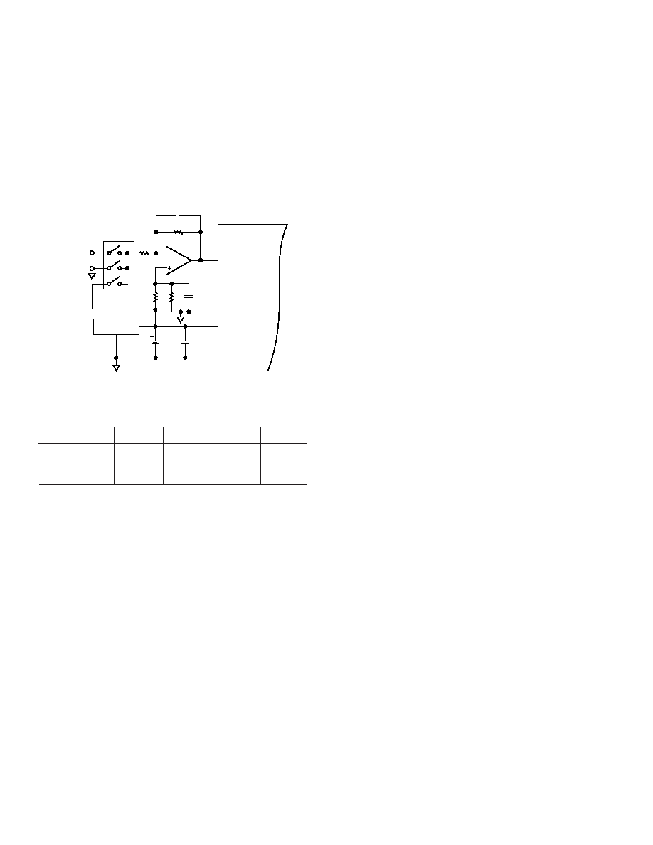
Figure 22 shows a connection diagram that allows this. Compo-
nent values required and resulting full-scale ranges are shown in
Table III.
U1
2.5V REF
ANALOG
INPUT
R2
R3
R4
100nF
R1
CF
U2
CREF
IN
INGND
REF
REFGND
100nF
AD7660
Figure 22. Using the AD7660 in 16-Bit Bipolar and/or
Wider Input Ranges
Table III. Component Values and Input Ranges
Input Range
R1 (k
W) R2 (kW)
R3 (k
W) R4 (kW)
±10 V
1
8
10
8
±5 V
1
4
10
6.67
0 V to –5 V
1
2
None
0
For bipolar range applications where accurate gain and offset
are desired, they can be calibrated by acquiring a ground and a
voltage reference using an analog multiplexer U2, as shown in
Figure 22. Also, CF can be used as a one-pole antialiasing filter.
Layout
The AD7660 has very good immunity to noise on the power
supplies as can be seen in Figure 9. However, care should still
be taken with regard to grounding layout.
The printed circuit board that houses the AD7660 should be
designed so the analog and digital sections are separated and
confined to certain areas of the board. This facilitates the use of
ground planes that can be easily separated. Digital and ana-
log ground planes should be joined in only one place,
preferably underneath the AD7660, or, at least, as close as
possible to the AD7660. If the AD7660 is in a system where
multiple devices require analog to digital ground connections,
the connection should still be made at one point only, a star
ground point that should be established as close as possible to
the AD7660.
It is recommended to avoid running digital lines under the device
as these will couple noise onto the die. The analog ground plane
should be allowed to run under the AD7660 to avoid noise
coupling. Fast switching signals like
CNVST or clocks should
be shielded with digital ground to avoid radiating noise to other
sections of the board and should never run near analog signal
paths. Crossover of digital and analog signals should be avoided.
Traces on different but close layers of the board should run at right
angles to each other. This will reduce the effect of feedthrough
through the board.
The power supply lines to the AD7660 should use as large a
trace as possible to provide low impedance paths and reduce the
effect of glitches on the power supply lines. Good decoupling is
also important to lower the supply’s impedance presented to the
AD7660 and to reduce the magnitude of the supply spikes.
Decoupling ceramic capacitors, typically 100 nF, should be placed
on each power supply pins AVDD, DVDD, and OVDD close to,
and ideally right up against, these pins and their corresponding
ground pins. Additionally, low ESR 10
mF capacitors should
be located in the vicinity of the ADC to further reduce low
frequency ripple.
The DVDD supply of the AD7660 can be either a separate
supply or come from the analog supply, AVDD, or from the
digital interface supply, OVDD. When the system digital supply
is noisy, or fast switching digital signals are present, it is recom-
mended if no separate supply is available, to connect the DVDD
digital supply to the analog supply AVDD through an RC filter as
shown in Figure 6 and to connect the system supply to the interface
digital supply OVDD and the remaining digital circuitry. When
DVDD is powered from the system supply, it is useful to insert
a bead to further reduce high frequency spikes.
The AD7660 has five different ground pins: INGND, REFGND,
AGND, DGND, and OGND. INGND is used to sense the
analog input signal. REFGND senses the reference voltage and
should be a low impedance return to the reference because it
carries pulsed currents. AGND is the ground to which most
internal ADC analog signals are referenced. This ground must be
connected with the least resistance to the analog ground plane.
DGND must be tied to the analog or digital ground plane depend-
ing on the configuration. OGND is connected to the digital
system ground.
Evaluating the AD7660 Performance
A recommended layout for the AD7660 is outlined in the
EVAL-AD7660 evaluation board for the AD7660. The evaluation
board package includes a fully assembled and tested evaluation
board, documentation, and software for controlling the board
from a PC via the EVAL-CONTROL-BRD2.
相关PDF资料 |
PDF描述 |
|---|---|
| VE-J11-MW-F1 | CONVERTER MOD DC/DC 12V 100W |
| LTC1403AIMSE#PBF | IC ADC 14BIT 2.8MSPS 10-MSOP |
| AD7658BSTZ | IC ADC 12BIT 6CH 250KSPS 64LQFP |
| AD7767BRUZ-1 | ADC 24BIT 64KSPS SAR 16-TSSOP |
| AD7714YRUZ | IC ADC SIGNAL COND 3/5V 24-TSSOP |
相关代理商/技术参数 |
参数描述 |
|---|---|
| AD7660ASTZ | 制造商:Analog Devices 功能描述:IC 16-BIT ADC |
| AD7660ASTZRL | 功能描述:IC ADC 16BIT UNIPOLAR 48LQFP RoHS:是 类别:集成电路 (IC) >> 数据采集 - 模数转换器 系列:PulSAR® 标准包装:1,000 系列:- 位数:12 采样率(每秒):300k 数据接口:并联 转换器数目:1 功率耗散(最大):75mW 电压电源:单电源 工作温度:0°C ~ 70°C 安装类型:表面贴装 封装/外壳:24-SOIC(0.295",7.50mm 宽) 供应商设备封装:24-SOIC 包装:带卷 (TR) 输入数目和类型:1 个单端,单极;1 个单端,双极 |
| AD7661 | 制造商:AD 制造商全称:Analog Devices 功能描述:14-Bit, 1 MSPS, Differential, Programmable Input PulSAR ADC |
| AD7661ACP | 制造商:Analog Devices 功能描述:ADC Single SAR 100ksps 16-bit Parallel/Serial 48-Pin LFCSP EP 制造商:Rochester Electronics LLC 功能描述:100KSPS, 16-BIT ADC INT REF, 2.5LSB - Bulk 制造商:Analog Devices 功能描述:16BIT ADC INT REF 7661 LFSCP-48 |
| AD7661ACPRL | 制造商:Analog Devices 功能描述:ADC Single SAR 100ksps 16-bit Parallel/Serial 48-Pin LFCSP EP T/R 制造商:Analog Devices 功能描述:ADC SGL SAR 100KSPS 16BIT PARALLEL/SERL 48LFCSP EP - Tape and Reel 制造商:Rochester Electronics LLC 功能描述:100KSPS, 16-BIT ADC INT REF, 2.5LSB - Tape and Reel |
发布紧急采购,3分钟左右您将得到回复。