- 您现在的位置:买卖IC网 > PDF目录10667 > AD7660ASTZ (Analog Devices Inc)IC ADC 16BIT UNIPOLAR 48-LQFP PDF资料下载
参数资料
| 型号: | AD7660ASTZ |
| 厂商: | Analog Devices Inc |
| 文件页数: | 6/20页 |
| 文件大小: | 0K |
| 描述: | IC ADC 16BIT UNIPOLAR 48-LQFP |
| 标准包装: | 1 |
| 系列: | PulSAR® |
| 位数: | 16 |
| 采样率(每秒): | 100k |
| 数据接口: | 串行,并联 |
| 转换器数目: | 1 |
| 功率耗散(最大): | 25mW |
| 电压电源: | 模拟和数字 |
| 工作温度: | -40°C ~ 85°C |
| 安装类型: | 表面贴装 |
| 封装/外壳: | 48-LQFP |
| 供应商设备封装: | 48-LQFP(7x7) |
| 包装: | 托盘 |
| 输入数目和类型: | 2 个伪差分,单极 |
| 产品目录页面: | 778 (CN2011-ZH PDF) |
| 配用: | EVAL-AD7660CBZ-ND - BOARD EVALUATION FOR AD7660 |
REV. D
AD7660
–14–
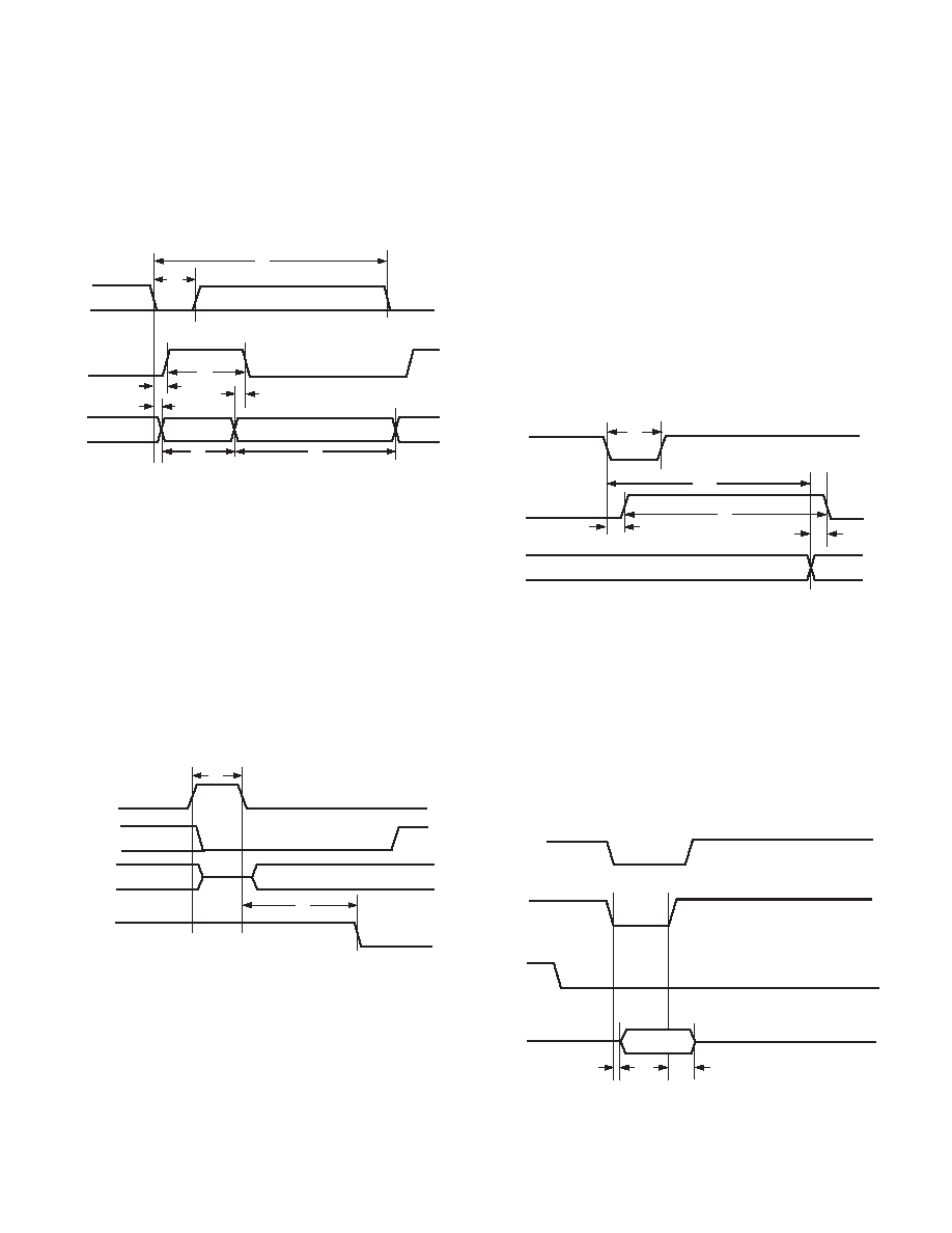
CONVERSION CONTROL
Figure 11 shows the detailed timing diagrams of the conversion
process. The AD7660 is controlled by the signal
CNVST, which
initiates conversion. Once initiated, it cannot be restarted or
aborted, even by the power-down input PD, until the conver-
sion is complete. The
CNVST signal operates independently of
CS and RD signals.
CNVST
BUSY
MODE
t2
t1
t3
t4
t5
t6
t7
t8
ACQUIRE
CONVERT
ACQUIRE
CONVERT
Figure 11. Basic Conversion Timing
For a true sampling application, the recommended operation of
the
CNVST signal is the following:
CNVST must be held HIGH from the previous falling edge
of BUSY, and during a minimum delay corresponding to the
acquisition time t8; then, when CNVST is brought LOW, a
conversion is initiated and the BUSY signal goes HIGH until
the completion of the conversion. Although
CNVST is a digital
signal, it should be designed with special care with fast, clean
edges and levels, with minimum overshoot and undershoot or
ringing. For applications where the SNR is critical, the
CNVST
signal should have a very low jitter. This may be achieved by
using a dedicated oscillator for
CNVST generation or, at least,
to clock it with a high frequency low jitter clock, as shown in
Figure 5.
t9
t8
RESET
DATABUS
BUSY
CNVST
Figure 12. RESET Timing
For other applications, conversions can be automatically initiated.
If
CNVST is held LOW when BUSY is LOW, the AD7660
controls the acquisition phase and then automatically initiates a
new conversion. By keeping
CNVST LOW, the AD7660 keeps
the conversion process running by itself. It should be noted that
the analog input has to be settled when BUSY goes LOW. Also,
at power-up,
CNVST should be brought LOW once to initiate
the conversion process. In this mode, the AD7660 could some-
times run slightly faster than the guaranteed limit of 100 kSPS.
DIGITAL INTERFACE
The AD7660 has a versatile digital interface; it can be interfaced
with the host system by using either a serial or parallel interface.
The serial interface is multiplexed on the parallel data bus. The
AD7660 digital interface also accommodates both 3 V or 5 V
logic by simply connecting the OVDD supply pin of the AD7660
to the host system interface digital supply. Finally, by using the
OB/
2C input pin, both twos complement or straight binary
coding can be used.
The two signals
CS and RD control the interface. CS and RD
have a similar effect because they are together internally. When
at least one of these signals is HIGH, the interface outputs are
in high impedance. Usually,
CS allows the selection of each
AD7660 in multicircuit applications and is held LOW in a
single AD7660 design.
RD is generally used to enable the con-
version result on the data bus.
t1
t3
t4
t11
CNVST
BUSY
DATA BUS
CS = RD = 0
t10
PREVIOUS CONVERSION DATA
NEW DATA
Figure 13. Master Parallel Data Timing for Reading
(Continuous Read)
PARALLEL INTERFACE
The AD7660 is configured to use the parallel interface when the
SER/
PAR is held LOW. The data can be read either after each
conversion, which is during the next acquisition phase, or during
the following conversion as shown, respectively, in Figures 14 and
15. When the data is read during the conversion, however, it is
recommended that it is read-only during the first half of the
conversion phase. This avoids any potential feedthrough between
voltage transients on the digital interface and the most critical
analog conversion circuitry.
CURRENT
CONVERSION
BUSY
DATA BUS
CS
RD
t12
t13
Figure 14. Slave Parallel Data Timing for Reading
(Read after Convert)
相关PDF资料 |
PDF描述 |
|---|---|
| VE-J11-MW-F1 | CONVERTER MOD DC/DC 12V 100W |
| LTC1403AIMSE#PBF | IC ADC 14BIT 2.8MSPS 10-MSOP |
| AD7658BSTZ | IC ADC 12BIT 6CH 250KSPS 64LQFP |
| AD7767BRUZ-1 | ADC 24BIT 64KSPS SAR 16-TSSOP |
| AD7714YRUZ | IC ADC SIGNAL COND 3/5V 24-TSSOP |
相关代理商/技术参数 |
参数描述 |
|---|---|
| AD7660ASTZ | 制造商:Analog Devices 功能描述:IC 16-BIT ADC |
| AD7660ASTZRL | 功能描述:IC ADC 16BIT UNIPOLAR 48LQFP RoHS:是 类别:集成电路 (IC) >> 数据采集 - 模数转换器 系列:PulSAR® 标准包装:1,000 系列:- 位数:12 采样率(每秒):300k 数据接口:并联 转换器数目:1 功率耗散(最大):75mW 电压电源:单电源 工作温度:0°C ~ 70°C 安装类型:表面贴装 封装/外壳:24-SOIC(0.295",7.50mm 宽) 供应商设备封装:24-SOIC 包装:带卷 (TR) 输入数目和类型:1 个单端,单极;1 个单端,双极 |
| AD7661 | 制造商:AD 制造商全称:Analog Devices 功能描述:14-Bit, 1 MSPS, Differential, Programmable Input PulSAR ADC |
| AD7661ACP | 制造商:Analog Devices 功能描述:ADC Single SAR 100ksps 16-bit Parallel/Serial 48-Pin LFCSP EP 制造商:Rochester Electronics LLC 功能描述:100KSPS, 16-BIT ADC INT REF, 2.5LSB - Bulk 制造商:Analog Devices 功能描述:16BIT ADC INT REF 7661 LFSCP-48 |
| AD7661ACPRL | 制造商:Analog Devices 功能描述:ADC Single SAR 100ksps 16-bit Parallel/Serial 48-Pin LFCSP EP T/R 制造商:Analog Devices 功能描述:ADC SGL SAR 100KSPS 16BIT PARALLEL/SERL 48LFCSP EP - Tape and Reel 制造商:Rochester Electronics LLC 功能描述:100KSPS, 16-BIT ADC INT REF, 2.5LSB - Tape and Reel |
发布紧急采购,3分钟左右您将得到回复。