参数资料
| 型号: | AD768AR |
| 厂商: | Analog Devices Inc |
| 文件页数: | 15/20页 |
| 文件大小: | 0K |
| 描述: | IC DAC 16BIT 30MSPS 28-SOIC |
| 产品培训模块: | Data Converter Fundamentals DAC Architectures |
| 标准包装: | 1 |
| 设置时间: | 25ns |
| 位数: | 16 |
| 数据接口: | 并联 |
| 转换器数目: | 1 |
| 电压电源: | 双 ± |
| 功率耗散(最大): | 600mW |
| 工作温度: | -40°C ~ 85°C |
| 安装类型: | 表面贴装 |
| 封装/外壳: | 28-SOIC(0.295",7.50mm 宽) |
| 供应商设备封装: | 28-SOIC W |
| 包装: | 管件 |
| 输出数目和类型: | 2 电流,单极;2 电流,双极 |
| 采样率(每秒): | 40M |
REV. B
–4–
AD768
WAFER TEST LIMITS1
Parameter
AD768ACHIPS Limit
Units
Integral Nonlinearity
2
±8
LSB max
Differential Nonlinearity
2
±6
LSB max
Offset Error
±0.2
% FSR max
Gain Error
±1.0
% FSR max
Reference Voltage
±1.0
% of nom. 2.5 V max
Positive Supply Current
40
mA max
Negative Supply Current
73
mA max
Power Dissipation
600
mW max
NOTES
1Electrical test are performed at wafer probe to the limits shown. Due to variations in assembly methods and normal
yield loss, yield after packaging is not guaranteed for standard product dice.
2Limits extrapolated from testing of individual bit errors.
3Die offers latch control pad. Edge triggered latches become level triggered when latch control and clock pads are high.
4Die substrate is connected to V
EE.
PIN DESCRIPTIONS
Pin No.
Symbol
Type
Name and Function
1
IOUTA
AO
DAC Current Output. Full-scale current when all data bits are 1s.
2
NR
AI
Noise Reduction Node. Add capacitor for noise reduction.
3
REFOUT
AO
Reference Output Voltage. Nominal value is 2.5 V.
4
NC
No Connect. Reserved for internal use.
5
REFCOM
P
Reference Ground.
6
IREFIN
AI
Reference Input Current. Nominal is 5 mA. DAC full-scale is 4
× this current.
7
DB0
DI
Data Bit 0 (LSB).
8–14
DB1–DB7
DI
Data Bits 1–7.
15
DCOM
P
Digital Ground.
16
CLOCK
DI
Clock Input. Data latched on positive edge of clock.
17–23
DB8–DB14
DI
Data Bits 8–14.
24
DB15
DI
Data Bit 15 (MSB).
25
VDD
P
Positive Supply Voltage. Nominal is +5 V.
26
VEE
P
Negative Supply Voltage. Nominal is –5 V.
27
IOUTB
AO
Complementary DAC Current Output. Full-scale current when all data bits are 0s.
28
LADCOM
P
DAC Ladder Common.
Type: AI = Analog Input; DI = Digital Input; AO = Analog Output; P = Power.
(TA = +25 C, VDD = +5.0 V, VEE = –5.0 V, IREFIN = 5 mA, unless otherwise noted)
VDD VDD
DB15
DB14 DB13
DB12 DB11
DB10
REFCOM IREFIN
DB0
DB1
DB2
DB3 DB4
VEE
IOUTB
LADCOM
IOUTA
NR
REFOUT
NC
DB9
DB8
CLOCK
LATCH CONTROL
DCOM
DB7
DB6
DB5
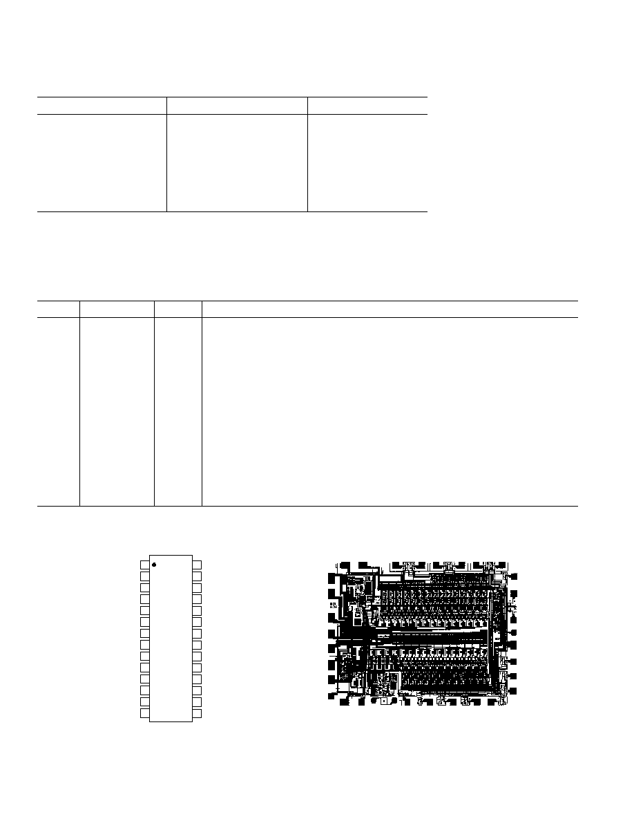
Die Size:
0.1106
× 0.1417 inch, 15,672 sq. mils
(2.81
× 3.60 mm, 10.116 sq. mm)
DICE CHARACTERISTICS
3, 4
PIN CONFIGURATION
14
13
12
11
17
16
15
20
19
18
10
9
8
1
2
3
4
7
6
5
TOP VIEW
(Not to Scale)
28
27
26
25
24
23
22
21
AD768
NC = NO CONNECT
IOUTA
VDD (+5V)
VEE (–5V)
IOUTB
LADCOM
NR
REFOUT
NC
DB13
DB14
DB15 (MSB)
REFCOM
IREFIN
(LSB) DB0
DB1
DB2
DB3
DB10
DB11
DB12
DB4
DB5
DB6
DB7
DB9
DCOM
CLOCK
DB8
相关PDF资料 |
PDF描述 |
|---|---|
| AD7724ASTZ | IC MOD SIGMA-DELTA DUAL 48LQFP |
| AD7729ARU | IC ADC 15BIT DUAL W/DAC 28-TSSOP |
| AD7746ARUZ | IC CONV 2CH CAP TO DGTL 16-TSSOP |
| AD7747ARUZ-REEL7 | IC CONV CAP TO DIG 24BIT 16TSSOP |
| AD7808BR | IC DAC 10BIT 3.3V OCTAL 24-SOIC |
相关代理商/技术参数 |
参数描述 |
|---|---|
| AD768AR-REEL | 制造商:Analog Devices 功能描述:DAC 1-CH R-2R/Current Steering 16-bit 28-Pin SOIC W T/R |
| AD768ARZ | 功能描述:IC DAC 16BIT 30MSPS 28-SOIC RoHS:是 类别:集成电路 (IC) >> 数据采集 - 数模转换器 系列:- 标准包装:1 系列:- 设置时间:4.5µs 位数:12 数据接口:串行,SPI? 转换器数目:1 电压电源:单电源 功率耗散(最大):- 工作温度:-40°C ~ 125°C 安装类型:表面贴装 封装/外壳:8-SOIC(0.154",3.90mm 宽) 供应商设备封装:8-SOICN 包装:剪切带 (CT) 输出数目和类型:1 电压,单极;1 电压,双极 采样率(每秒):* 其它名称:MCP4921T-E/SNCTMCP4921T-E/SNRCTMCP4921T-E/SNRCT-ND |
| AD768ARZ-REEL | 功能描述:IC DAC 16BIT 30MSPS 28-SOIC RoHS:是 类别:集成电路 (IC) >> 数据采集 - 数模转换器 系列:- 产品培训模块:Data Converter Fundamentals DAC Architectures 标准包装:750 系列:- 设置时间:7µs 位数:16 数据接口:并联 转换器数目:1 电压电源:双 ± 功率耗散(最大):100mW 工作温度:0°C ~ 70°C 安装类型:表面贴装 封装/外壳:28-LCC(J 形引线) 供应商设备封装:28-PLCC(11.51x11.51) 包装:带卷 (TR) 输出数目和类型:1 电压,单极;1 电压,双极 采样率(每秒):143k |
| AD768-EB | 制造商:Analog Devices 功能描述:IC, 16-BIT 32 MSPS DAC - Bulk |
| AD768-EBZ | 制造商:Analog Devices 功能描述:EVAL BOARD - Boxed Product (Development Kits) |
发布紧急采购,3分钟左右您将得到回复。