参数资料
| 型号: | AD768AR |
| 厂商: | Analog Devices Inc |
| 文件页数: | 19/20页 |
| 文件大小: | 0K |
| 描述: | IC DAC 16BIT 30MSPS 28-SOIC |
| 产品培训模块: | Data Converter Fundamentals DAC Architectures |
| 标准包装: | 1 |
| 设置时间: | 25ns |
| 位数: | 16 |
| 数据接口: | 并联 |
| 转换器数目: | 1 |
| 电压电源: | 双 ± |
| 功率耗散(最大): | 600mW |
| 工作温度: | -40°C ~ 85°C |
| 安装类型: | 表面贴装 |
| 封装/外壳: | 28-SOIC(0.295",7.50mm 宽) |
| 供应商设备封装: | 28-SOIC W |
| 包装: | 管件 |
| 输出数目和类型: | 2 电流,单极;2 电流,双极 |
| 采样率(每秒): | 40M |

REV. B
–8–
AD768
DIGITAL INPUT CODE – k
8
–8
065
10
20
30
40
4
–2
–4
–6
6
0
2
DNL
ERROR
–
LSB
50
60
5
152535
4555
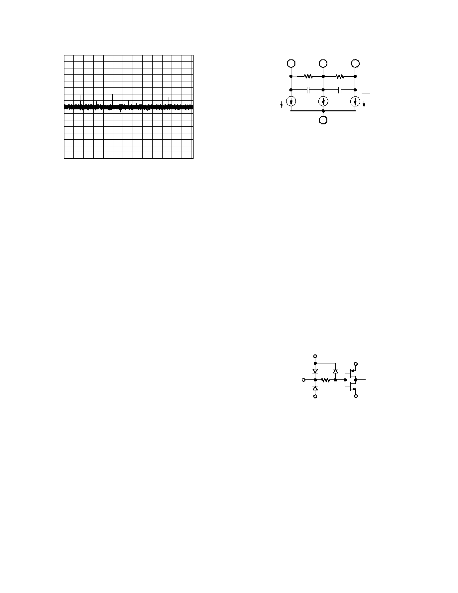
Figure 9. Typical DNL Performance
The outputs have a compliance range of –1.2 V to +5.0 V with
respect to LADCOM. The current steering output stages will
remain functional over this range. Operation beyond the maxi-
mum compliance limits may cause either output stage saturation
or breakdown, resulting in nonlinear performance. The rated dc
and ac performance specifications are for an output voltage of
0 V to –1 V.
The current in LADCOM is proportional to IREFIN and has been
carefully configured to be independent of digital code when the
output is connected to a virtual ground. This minimizes any det-
rimental effects of ladder ground resistance on linearity. For
optimal dc linearity, IOUTA should be connected directly to a
virtual ground, and IOUTB should be grounded. An example of
this configuration is provided in the section “Buffered Voltage
Output.” If IOUTA is driving a resistive load directly, then
IOUTB should be terminated with an equal impedance. This
will ensure the current in LADCOM remains constant with digi-
tal code, and is recommended for improved dc linearity in the
unbuffered voltage output configuration.
As shown in Figure 10, there is an equivalent output impedance
of 1 k
in parallel with 3 pF at each output terminal. If the out-
put voltage deviates from the ladder common voltage, an error
current flows through this 1 k
impedance. This is a linear effect
which does not change with input code, so it appears as a gain
error. With 50
output termination, the resulting gain error is
approximately –5%. An example of this configuration is pro-
vided in the section Unbuffered Voltage Output.
1
26
27
28
1k
1k
3pF
IOUT
IREFIN
x2.75
VEE
LADCOM
IOUTB
IOUTA
Figure 10. Equivalent Analog Output Circuit
DIGITAL INPUTS
The AD768 digital inputs consist of 16 data input pins and a
clock pin. The 16-bit parallel data inputs follow standard posi-
tive binary coding, where DB15 is the most significant bit
(MSB) and DB0 is the least significant bit (LSB). IOUTA pro-
duces full-scale output current when all data bits are at logic 1.
IOUTB is the complementary output, with full-scale when all
data bits are at logic 0. The full-scale current is split between
the two outputs as a function of the input code.
The digital interface is implemented using an edge-triggered
master slave latch. The DAC output is updated following the
rising edge of the clock, and is designed to support a clock rate
as high as 40 MSPS. The clock can be operated at any duty
cycle that meets the specified minimum latch pulse width. The
setup and hold times can also be varied within the clock cycle as
long as the specified minimums are met, although the location
of these transition edges may affect digital feedthrough. The
digital inputs are CMOS compatible with logic thresholds set to
approximately half the positive supply voltage. The small input
current requirements allow for easy interfacing to unbuffered
CMOS logic. Figure 11 shows the equivalent digital input
circuit.
VCC
VEE
DIGITAL
INPUT
VCC
DCOM
Figure 11. Equivalent Digital Input Circuit
Digital input signals to the DAC should be isolated from the
analog output as much as possible. Interconnect distances to the
DAC inputs should be kept as short as possible. Termination
resistors may improve performance if the digital lines become
too long. To minimize digital feedthrough, the inputs should be
free from glitches and ringing, and may be further improved
with a reduction of edge speed.
相关PDF资料 |
PDF描述 |
|---|---|
| AD7724ASTZ | IC MOD SIGMA-DELTA DUAL 48LQFP |
| AD7729ARU | IC ADC 15BIT DUAL W/DAC 28-TSSOP |
| AD7746ARUZ | IC CONV 2CH CAP TO DGTL 16-TSSOP |
| AD7747ARUZ-REEL7 | IC CONV CAP TO DIG 24BIT 16TSSOP |
| AD7808BR | IC DAC 10BIT 3.3V OCTAL 24-SOIC |
相关代理商/技术参数 |
参数描述 |
|---|---|
| AD768AR-REEL | 制造商:Analog Devices 功能描述:DAC 1-CH R-2R/Current Steering 16-bit 28-Pin SOIC W T/R |
| AD768ARZ | 功能描述:IC DAC 16BIT 30MSPS 28-SOIC RoHS:是 类别:集成电路 (IC) >> 数据采集 - 数模转换器 系列:- 标准包装:1 系列:- 设置时间:4.5µs 位数:12 数据接口:串行,SPI? 转换器数目:1 电压电源:单电源 功率耗散(最大):- 工作温度:-40°C ~ 125°C 安装类型:表面贴装 封装/外壳:8-SOIC(0.154",3.90mm 宽) 供应商设备封装:8-SOICN 包装:剪切带 (CT) 输出数目和类型:1 电压,单极;1 电压,双极 采样率(每秒):* 其它名称:MCP4921T-E/SNCTMCP4921T-E/SNRCTMCP4921T-E/SNRCT-ND |
| AD768ARZ-REEL | 功能描述:IC DAC 16BIT 30MSPS 28-SOIC RoHS:是 类别:集成电路 (IC) >> 数据采集 - 数模转换器 系列:- 产品培训模块:Data Converter Fundamentals DAC Architectures 标准包装:750 系列:- 设置时间:7µs 位数:16 数据接口:并联 转换器数目:1 电压电源:双 ± 功率耗散(最大):100mW 工作温度:0°C ~ 70°C 安装类型:表面贴装 封装/外壳:28-LCC(J 形引线) 供应商设备封装:28-PLCC(11.51x11.51) 包装:带卷 (TR) 输出数目和类型:1 电压,单极;1 电压,双极 采样率(每秒):143k |
| AD768-EB | 制造商:Analog Devices 功能描述:IC, 16-BIT 32 MSPS DAC - Bulk |
| AD768-EBZ | 制造商:Analog Devices 功能描述:EVAL BOARD - Boxed Product (Development Kits) |
发布紧急采购,3分钟左右您将得到回复。