- 您现在的位置:买卖IC网 > PDF目录1982 > AD7699BCPZRL7 (Analog Devices Inc)IC ADC 8CH 16BIT 500KSPS 20LFCSP PDF资料下载
参数资料
| 型号: | AD7699BCPZRL7 |
| 厂商: | Analog Devices Inc |
| 文件页数: | 8/28页 |
| 文件大小: | 0K |
| 描述: | IC ADC 8CH 16BIT 500KSPS 20LFCSP |
| 标准包装: | 1,500 |
| 位数: | 16 |
| 采样率(每秒): | 500k |
| 数据接口: | DSP,MICROWIRE?,QSPI?,串行,SPI? |
| 转换器数目: | 1 |
| 功率耗散(最大): | 32mW |
| 电压电源: | 模拟和数字 |
| 工作温度: | -40°C ~ 85°C |
| 安装类型: | 表面贴装 |
| 封装/外壳: | 20-VFQFN 裸露焊盘,CSP |
| 供应商设备封装: | 20-LFCSP-VQ |
| 包装: | 带卷 (TR) |
| 输入数目和类型: | 8 个单端,单极;4 个差分,单极;4 个差分,双极;4 个伪差分,双极 |
第1页第2页第3页第4页第5页第6页第7页当前第8页第9页第10页第11页第12页第13页第14页第15页第16页第17页第18页第19页第20页第21页第22页第23页第24页第25页第26页第27页第28页
AD7699
Data Sheet
Rev.
| Page 16 of 28
Unipolar or Bipolar
Figure 27 shows an example of the recommended connection
diagram for the AD7699 when multiple supplies are available.
Bipolar Single Supply
Figure 28 shows an example of a system with a bipolar input
using single supplies with the internal reference (optional
different VIO supply). This circuit is also useful when the
amplifier/signal conditioning circuit is remotely located with
some common mode present. Note that for any input config-
uration, the inputs, INx, are unipolar and always referenced to
GND (no negative voltages even in bipolar range).
For this circuit, a rail-to-rail input/output amplifier can be used;
however, the offset voltage vs. input common-mode range should
be noted and taken into consideration (1 LSB = 62.5 μV with
VREF = 4.096 V). Note that the conversion results are in twos
complement format when using the bipolar input configuration.
Refer to the AN-581 Application Note, Biasing and Decoupling
Op Amps in Single Supply Applications, at www.analog.com for
additional details about using single-supply amplifiers.
ANALOG INPUTS
Input Structure
Figure 29 shows an equivalent circuit of the input structure of
the AD7699. The two diodes, D1 and D2, provide ESD
protection for the analog inputs, IN[7:0] and COM. Care must
be taken to ensure that the analog input signal does not exceed
the supply rails by more than 0.3 V because this causes the
diodes to become forward-biased and to start conducting
current.
These diodes can handle a forward-biased current of 130 mA
maximum. For instance, these conditions may eventually occur
when the input buffer supplies are different from VDD. In such
a case, for example, an input buffer with a short circuit, the
current limitation can be used to protect the part.
CIN
RIN
D1
D2
CPIN
INx+
OR INx–
OR COM
GND
VDD
07
35
4-
0
27
Figure 29. Equivalent Analog Input Circuit
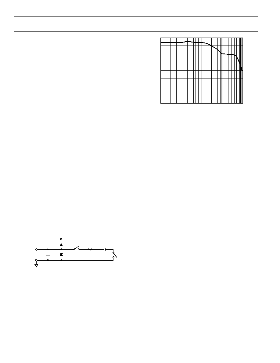
This analog input structure allows the sampling of the true
differential signal between INx+ and COM or INx+ and INx.
(COM or INx = GND ± 0.1 V or VREF ± 0.1 V). By using these
differential inputs, signals common to both inputs are rejected,
as shown in Figure 30.
70
65
60
55
50
45
40
35
30
1
10k
10
CM
RR
(
d
B)
100
1k
FREQUENCY (kHz)
07
35
4-
02
8
Figure 30. Analog Input CMRR vs. Frequency
During the acquisition phase, the impedance of the analog inputs
can be modeled as a parallel combination of the capacitor, CPIN,
and the network formed by the series connection of RIN and CIN.
CPIN is primarily the pin capacitance. RIN is typically 400 Ω (8.8 kΩ
when the one-pole filter is active) and is a lumped component
made up of serial resistors and the on resistance of the switches.
CIN is typically 27 pF and is mainly the ADC sampling capacitor.
Selectable Low-Pass Filter
During the conversion phase, where the switches are opened,
the input impedance is limited to CPIN. While the AD7699 is
acquiring, RIN and CIN make a one-pole, low-pass filter that
reduces undesirable aliasing effects and limits the noise from
the driving circuitry. The low-pass filter can be programmed
for the full bandwidth or of the bandwidth with CFG[6], as
shown in Table 8. Note that the converter throughput must also be
reduced by when using the filter. If the maximum throughput
is used with the BW set to , the acquisition time of the
converter, tACQ, is violated, resulting in poor THD.
Input Configurations
Figure 31 shows the different methods for configuring the analog
inputs with the configuration register (CFG[12:10]). Refer to
the Configuration Register, CFG section for more details.
B
相关PDF资料 |
PDF描述 |
|---|---|
| AD7701BN | IC ADC 16BIT LC2MOS MONO 20-DIP |
| AD7703BN | IC ADC 20BIT LC2MOS 20-DIP |
| AD7706BN | IC ADC 16BIT 3CH 16-DIP |
| AD7707BRU | IC ADC 16BIT 3CH 20-TSSOP |
| AD7709ARU | IC ADC 16BIT SIGMA-DELTA 24TSSOP |
相关代理商/技术参数 |
参数描述 |
|---|---|
| AD7701 | 制造商:AD 制造商全称:Analog Devices 功能描述:LC2MOS 16-Bit A/D Converter |
| AD7701AN | 功能描述:IC ADC 16BIT LC2MOS 20-DIP RoHS:否 类别:集成电路 (IC) >> 数据采集 - 模数转换器 系列:- 标准包装:1 系列:- 位数:14 采样率(每秒):83k 数据接口:串行,并联 转换器数目:1 功率耗散(最大):95mW 电压电源:双 ± 工作温度:0°C ~ 70°C 安装类型:通孔 封装/外壳:28-DIP(0.600",15.24mm) 供应商设备封装:28-PDIP 包装:管件 输入数目和类型:1 个单端,双极 |
| AD7701ANZ | 功能描述:IC ADC 16BIT LC2MOS 20-DIP RoHS:是 类别:集成电路 (IC) >> 数据采集 - 模数转换器 系列:- 标准包装:1 系列:microPOWER™ 位数:8 采样率(每秒):1M 数据接口:串行,SPI? 转换器数目:1 功率耗散(最大):- 电压电源:模拟和数字 工作温度:-40°C ~ 125°C 安装类型:表面贴装 封装/外壳:24-VFQFN 裸露焊盘 供应商设备封装:24-VQFN 裸露焊盘(4x4) 包装:Digi-Reel® 输入数目和类型:8 个单端,单极 产品目录页面:892 (CN2011-ZH PDF) 其它名称:296-25851-6 |
| AD7701AQ | 制造商:AD 制造商全称:Analog Devices 功能描述:LC2MOS 16-Bit A/D Converter |
| AD7701AR | 功能描述:IC ADC 16BIT LC2MOS 20-SOIC RoHS:否 类别:集成电路 (IC) >> 数据采集 - 模数转换器 系列:- 标准包装:1 系列:- 位数:14 采样率(每秒):83k 数据接口:串行,并联 转换器数目:1 功率耗散(最大):95mW 电压电源:双 ± 工作温度:0°C ~ 70°C 安装类型:通孔 封装/外壳:28-DIP(0.600",15.24mm) 供应商设备封装:28-PDIP 包装:管件 输入数目和类型:1 个单端,双极 |
发布紧急采购,3分钟左右您将得到回复。