- 您现在的位置:买卖IC网 > PDF目录10118 > AD7701AR (Analog Devices Inc)IC ADC 16BIT LC2MOS 20-SOIC PDF资料下载
参数资料
| 型号: | AD7701AR |
| 厂商: | Analog Devices Inc |
| 文件页数: | 2/20页 |
| 文件大小: | 0K |
| 描述: | IC ADC 16BIT LC2MOS 20-SOIC |
| 标准包装: | 1 |
| 位数: | 16 |
| 采样率(每秒): | 4k |
| 数据接口: | 串行 |
| 转换器数目: | 1 |
| 功率耗散(最大): | 37mW |
| 电压电源: | 模拟和数字,双 ± |
| 工作温度: | -40°C ~ 85°C |
| 安装类型: | 表面贴装 |
| 封装/外壳: | 20-SOIC(0.295",7.50mm 宽) |
| 供应商设备封装: | 20-SOIC W |
| 包装: | 管件 |
| 输入数目和类型: | 1 个单端,单极;1 个单端,双极 |
REV. E
–10–
AD7701
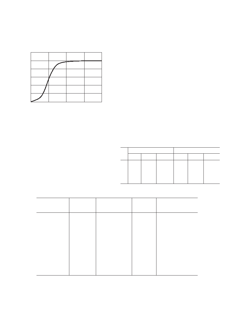
The output settling of the AD7701 in response to a step input
change is shown in Figure 12. The Gaussian response has fast
settling with no overshoot, and the worst-case settling time to
± 0.0007% (± 0.5 LSB) is 125 ms with a 4.096 MHz master
clock frequency.
PERCENT
OF
FINAL
VALUE
100
80
60
40
20
0
040
80
120
160
TIME – ms
Figure 12. AD7701 Step Response
USING THE AD7701
SYSTEM DESIGN CONSIDERATIONS
The AD7701 operates differently from successive approxima-
tion ADCs or other integrating ADCs. Since it samples the
signal continuously, like a tracking ADC, there is no need for a
start convert command. The 16-bit output register is updated at
a 4 kHz rate, and the output can be read at any time, either
synchronously or asynchronously.
CLOCKING
The AD7701 requires a master clock input, which may be an
external TTL/CMOS compatible clock signal applied to the
CLKIN pin (CLKOUT not used). Alternatively, a crystal of
the correct frequency can be connected between CLKIN and
CLKOUT, when the clock circuit will function as a crystal
controlled oscillator.
The input sampling frequency, output data rate, filter character-
istics, and calibration time are all directly related to the master
clock frequency, fCLKIN, by the ratios given in the specification
table. Therefore, the first step in system design with the AD7701 is
to select a master clock frequency suitable for the bandwidth
and output data rate required by the application.
ANALOG INPUT RANGES
The AD7701 performs conversion relative to an externally
supplied reference voltage that allows easy interfacing to
ratiometric systems. In addition, either unipolar or bipolar input
voltage ranges may be selected using the BP/
UP input. With
BP/
UP tied low, the input range is unipolar and the span is 0 to
+VREF. With BP/UP tied high, the input range is bipolar and the
span is
±VREF. In the Bipolar mode, both positive and negative
full scale are directly determined by VREF. This offers superior
tracking of positive and negative full scale and better midscale
(bipolar zero) stability than bipolar schemes that simply scale
and offset the input range.
The digital output coding for the unipolar range is unipolar
binary; for the bipolar range it is offset binary. Bit weights for
the Unipolar and Bipolar modes are shown in Table I. The
input voltages and output codes for unipolar and bipolar ranges,
using the recommended +2.5 V reference, are shown in
Table II.
Table I. Bit Weight Table (2.5 V Reference Voltage)
Unipolar Mode
Bipolar Mode
V
LSBs
% FS
ppm FS
LSBs
% FS
ppm FS
10
0.26
0.0004
4
0.13
0.0002
2
19
0.5
0.0008
8
0.26
0.0004
4
38
1.00
0.0015
15
0.5
0.0008
8
76
2.00
0.0031
31
1.00
0.0015
15
153
4.00
0.0061
61
2.00
0.0031
31
Table II. Output Coding
Unipolar Mode
Bipolar Mode
Input Relative to
FS and AGND
Input (V)
FS and AGND
Input (V)
Output Data
1111 1111 1111 1111
+VREF – 1.5 LSB
+2.499943
+VREF – 1.5 LSB
+2.499886
1111 1111 1111 1110
+VREF – 2.5 LSB
+2.499905
+VREF – 2.5 LSB
+2.499810
1111 1111 1111 1101
+VREF – 3.5 LSB
+2.499867
+VREF – 3.5 LSB
+2.499733
1111 1111 1111 1100
1000 0000 0000 0001
+VREF/2 + 0.5 LSB
+1.250019
AGND + 0.5 LSB
+0.000038
1000 0000 0000 0000
+VREF/2 – 0.5 LSB
+1.249981
AGND – 0.5 LSB
–0.000038
0111 1111 1111 1111
+VREF/2 – 1.5 LSB
+1.249943
AGND – 1.5 LSB
–0.000114
0111 1111 1111 1110
0000 0000 0000 0011
AGND + 2.5 LSB
+0.000095
–VREF + 2.5 LSB
–2.499810
0000 0000 0000 0010
AGND + 1.5 LSB
+0.000057
–VREF + 1.5 LSB
–2.499886
0000 0000 0000 0001
AGND + 0.5 LSB
+0.000019
–VREF + 0.5 LSB
–2.499962
0000 0000 0000 0000
NOTES
1. VREF = 2.5 V
2. AGND = 0 V
3. Unipolar Mode, 1 LSB = 2.5 V/655536 = 0.000038 V
4. Bipolar Mode, 1 LSB = 5 V/65536 = 0.000076 V
5. Inputs are voltages at code transitions.
相关PDF资料 |
PDF描述 |
|---|---|
| D38999/24FE26PA | CONN RCPT 26POS JAM NUT W/PINS |
| VI-2NR-MX-F2 | CONVERTER MOD DC/DC 7.5V 75W |
| AD7713ARZ-REEL | IC ADC 24BIT SIGMA-DELTA 24SOIC |
| MS27467T9B44S | CONN PLUG 4POS STRAIGHT W/SCKT |
| AD977CRZ | IC ADC 16BIT 100KSPS 20SOIC |
相关代理商/技术参数 |
参数描述 |
|---|---|
| AD7701AR-REEL | 制造商:Rochester Electronics LLC 功能描述:- Tape and Reel |
| AD7701ARS | 功能描述:IC ADC 16BIT LC2MOS MONO 28-SSOP RoHS:否 类别:集成电路 (IC) >> 数据采集 - 模数转换器 系列:- 标准包装:1 系列:- 位数:14 采样率(每秒):83k 数据接口:串行,并联 转换器数目:1 功率耗散(最大):95mW 电压电源:双 ± 工作温度:0°C ~ 70°C 安装类型:通孔 封装/外壳:28-DIP(0.600",15.24mm) 供应商设备封装:28-PDIP 包装:管件 输入数目和类型:1 个单端,双极 |
| AD7701ARS-REEL | 功能描述:IC ADC 16BIT LC2MOS MONO 28-SSOP RoHS:否 类别:集成电路 (IC) >> 数据采集 - 模数转换器 系列:- 标准包装:1 系列:- 位数:14 采样率(每秒):83k 数据接口:串行,并联 转换器数目:1 功率耗散(最大):95mW 电压电源:双 ± 工作温度:0°C ~ 70°C 安装类型:通孔 封装/外壳:28-DIP(0.600",15.24mm) 供应商设备封装:28-PDIP 包装:管件 输入数目和类型:1 个单端,双极 |
| AD7701ARSZ | 功能描述:IC ADC 16BIT LC2MOS MONO 28SSOP RoHS:是 类别:集成电路 (IC) >> 数据采集 - 模数转换器 系列:- 标准包装:1 系列:- 位数:14 采样率(每秒):83k 数据接口:串行,并联 转换器数目:1 功率耗散(最大):95mW 电压电源:双 ± 工作温度:0°C ~ 70°C 安装类型:通孔 封装/外壳:28-DIP(0.600",15.24mm) 供应商设备封装:28-PDIP 包装:管件 输入数目和类型:1 个单端,双极 |
| AD7701ARSZ-REEL | 功能描述:IC ADC 16BIT LC2MOS MONO 28SSOP RoHS:是 类别:集成电路 (IC) >> 数据采集 - 模数转换器 系列:- 标准包装:1,000 系列:- 位数:12 采样率(每秒):300k 数据接口:并联 转换器数目:1 功率耗散(最大):75mW 电压电源:单电源 工作温度:0°C ~ 70°C 安装类型:表面贴装 封装/外壳:24-SOIC(0.295",7.50mm 宽) 供应商设备封装:24-SOIC 包装:带卷 (TR) 输入数目和类型:1 个单端,单极;1 个单端,双极 |
发布紧急采购,3分钟左右您将得到回复。