- 您现在的位置:买卖IC网 > PDF目录10118 > AD7701AR (Analog Devices Inc)IC ADC 16BIT LC2MOS 20-SOIC PDF资料下载
参数资料
| 型号: | AD7701AR |
| 厂商: | Analog Devices Inc |
| 文件页数: | 4/20页 |
| 文件大小: | 0K |
| 描述: | IC ADC 16BIT LC2MOS 20-SOIC |
| 标准包装: | 1 |
| 位数: | 16 |
| 采样率(每秒): | 4k |
| 数据接口: | 串行 |
| 转换器数目: | 1 |
| 功率耗散(最大): | 37mW |
| 电压电源: | 模拟和数字,双 ± |
| 工作温度: | -40°C ~ 85°C |
| 安装类型: | 表面贴装 |
| 封装/外壳: | 20-SOIC(0.295",7.50mm 宽) |
| 供应商设备封装: | 20-SOIC W |
| 包装: | 管件 |
| 输入数目和类型: | 1 个单端,单极;1 个单端,双极 |
REV. E
–12–
AD7701
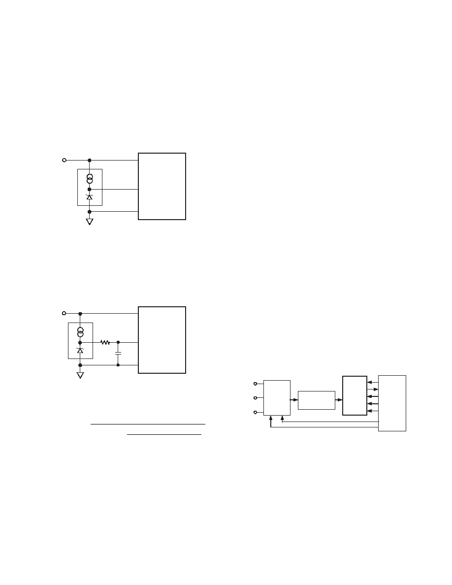
VOLTAGE REFERENCE CONNECTIONS
The voltage applied to the VREF pin defines the analog input
range. The specified reference voltage is 2.5 V, but the AD7701
will operate with reference voltages from 1 V to 3 V with little
degradation in performance.
The reference input presents exactly the same dynamic load as
the analog input, but in the case of the reference input, source
resistance and long settling time introduce gain errors rather
than offset errors. Fortunately, most precision references have
sufficiently low output impedance and wide enough bandwidth
to settle to 10
V within 62 clock cycles.
AGND
AD7701
+5V
AVDD
VREF
LT1019
Figure 14. Typical External Reference Connections
The digital filter of the AD7701 removes noise from the refer-
ence input, just as it does with noise at the analog input, and the
same limitations apply regarding lack of noise rejection at inte-
ger multiples of the sampling frequency. If reference noise is a
problem, some voltage references offer noise reduction schemes
using an external capacitor. Alternatively, a simple RC filter
may be used, as shown in Figure 15.
+5V
AD580
AGND
AD7701
AVDD
VREF
RF
13k
CF
100pF
Figure 15. Filtered Reference Input
The same considerations apply to this filter as to a filter at the
analog input. In this case:
[RF(CF
+10 pF)]=
62
f CLKIN
× ln
100 mV
×C
IN (CIN
+C
F )
V FSE
where
fCLKIN is the master clock frequency.
VFSE is the maximum desired error in volts.
GROUNDING AND SUPPLY DECOUPLING
AGND is the ground reference voltage for the AD7701 and is
completely independent of DGND. Any noise riding on the
AGND input with respect to the system analog ground will
cause conversion errors. AGND should, therefore, be used as
the system ground and also as the ground for the analog input
and reference voltage.
The analog and digital power supplies to the AD7701 are inde-
pendent and separately pinned out to minimize coupling between
analog and digital sections of the device. The digital filter will
provide rejections of broadband noise on the power supplies,
except at integer multiples of the sampling frequency. Therefore,
the two analog supplies should be decoupled to AGND using
100 nF ceramic capacitors to provide power supply noise rejec-
tions at these frequencies. The two digital supplies should similarly
be decoupled to DGND.
ACCURACY AND AUTOCALIBRATION
Sigma-delta ADCs, like VFCs and other integrating ADCs, do
not contain any source of nonmonotonicity and inherently offer
no-missing-codes performance. The AD7701 achieves excellent
linearity (
±0.0007%) by the use of high quality, on-chip silicon
dioxide capacitors, which have a very low capacitance/voltage
coefficient.
The AD7701 offers two self-calibration modes using the on-chip
calibration microcontroller and SRAM. Table III is a truth table
for the calibration control inputs SC1 and SC2.
In the self-calibration mode, zero scale is calibrated against the
AGND pin and full scale is calibrated against the VREF pin, to
remove internal errors.
Note that in the Bipolar mode the AD7701 calibrates positive
full scale and midscale (bipolar zero).
In the system-calibration mode, the AD7701 calibrates its zero
and full scale to voltages present on the analog input pin in two
sequential steps. This allows system offsets and/or gain errors to
be nulled out.
SYSTEM
REF HI
AIN
SYSTEM
REF LO
ANALOG
MUX
A0
A1
SIGNAL
CONDITIONING
AD7701
SCLK
SDATA
CAL
SC1
SC2
MICRO-
COMPUTER
Figure 16. Typical Connections for System Calibration
A typical system calibration scheme is shown in Figure 16. In
normal operation, the analog signal is fed to the AD7701 via an
analog multiplexer. When the system is to be calibrated, AIN is
first switched to the system REF LO via the multiplexer and
CAL is strobed high, with SC1 and SC2 both high. AIN is then
switched to the system REF HI and CAL is strobed, with SC1
low and SC2 high. In this way, the effect of all error sources
相关PDF资料 |
PDF描述 |
|---|---|
| D38999/24FE26PA | CONN RCPT 26POS JAM NUT W/PINS |
| VI-2NR-MX-F2 | CONVERTER MOD DC/DC 7.5V 75W |
| AD7713ARZ-REEL | IC ADC 24BIT SIGMA-DELTA 24SOIC |
| MS27467T9B44S | CONN PLUG 4POS STRAIGHT W/SCKT |
| AD977CRZ | IC ADC 16BIT 100KSPS 20SOIC |
相关代理商/技术参数 |
参数描述 |
|---|---|
| AD7701AR-REEL | 制造商:Rochester Electronics LLC 功能描述:- Tape and Reel |
| AD7701ARS | 功能描述:IC ADC 16BIT LC2MOS MONO 28-SSOP RoHS:否 类别:集成电路 (IC) >> 数据采集 - 模数转换器 系列:- 标准包装:1 系列:- 位数:14 采样率(每秒):83k 数据接口:串行,并联 转换器数目:1 功率耗散(最大):95mW 电压电源:双 ± 工作温度:0°C ~ 70°C 安装类型:通孔 封装/外壳:28-DIP(0.600",15.24mm) 供应商设备封装:28-PDIP 包装:管件 输入数目和类型:1 个单端,双极 |
| AD7701ARS-REEL | 功能描述:IC ADC 16BIT LC2MOS MONO 28-SSOP RoHS:否 类别:集成电路 (IC) >> 数据采集 - 模数转换器 系列:- 标准包装:1 系列:- 位数:14 采样率(每秒):83k 数据接口:串行,并联 转换器数目:1 功率耗散(最大):95mW 电压电源:双 ± 工作温度:0°C ~ 70°C 安装类型:通孔 封装/外壳:28-DIP(0.600",15.24mm) 供应商设备封装:28-PDIP 包装:管件 输入数目和类型:1 个单端,双极 |
| AD7701ARSZ | 功能描述:IC ADC 16BIT LC2MOS MONO 28SSOP RoHS:是 类别:集成电路 (IC) >> 数据采集 - 模数转换器 系列:- 标准包装:1 系列:- 位数:14 采样率(每秒):83k 数据接口:串行,并联 转换器数目:1 功率耗散(最大):95mW 电压电源:双 ± 工作温度:0°C ~ 70°C 安装类型:通孔 封装/外壳:28-DIP(0.600",15.24mm) 供应商设备封装:28-PDIP 包装:管件 输入数目和类型:1 个单端,双极 |
| AD7701ARSZ-REEL | 功能描述:IC ADC 16BIT LC2MOS MONO 28SSOP RoHS:是 类别:集成电路 (IC) >> 数据采集 - 模数转换器 系列:- 标准包装:1,000 系列:- 位数:12 采样率(每秒):300k 数据接口:并联 转换器数目:1 功率耗散(最大):75mW 电压电源:单电源 工作温度:0°C ~ 70°C 安装类型:表面贴装 封装/外壳:24-SOIC(0.295",7.50mm 宽) 供应商设备封装:24-SOIC 包装:带卷 (TR) 输入数目和类型:1 个单端,单极;1 个单端,双极 |
发布紧急采购,3分钟左右您将得到回复。