- 您现在的位置:买卖IC网 > PDF目录10292 > AD7705BRZ-REEL7 (Analog Devices Inc)IC ADC 16BIT 2CHAN 16SOIC PDF资料下载
参数资料
| 型号: | AD7705BRZ-REEL7 |
| 厂商: | Analog Devices Inc |
| 文件页数: | 42/44页 |
| 文件大小: | 0K |
| 描述: | IC ADC 16BIT 2CHAN 16SOIC |
| 标准包装: | 1 |
| 位数: | 16 |
| 采样率(每秒): | 500 |
| 数据接口: | DSP,MICROWIRE?,QSPI?,串行,SPI? |
| 转换器数目: | 1 |
| 功率耗散(最大): | 1mW |
| 电压电源: | 单电源 |
| 工作温度: | -40°C ~ 85°C |
| 安装类型: | 表面贴装 |
| 封装/外壳: | 16-SOIC(0.295",7.50mm 宽) |
| 供应商设备封装: | 16-SOIC W |
| 包装: | 标准包装 |
| 输入数目和类型: | 2 个差分,单极;2 个差分,双极 |
| 其它名称: | AD7705BRZ-REEL7DKR |
第1页第2页第3页第4页第5页第6页第7页第8页第9页第10页第11页第12页第13页第14页第15页第16页第17页第18页第19页第20页第21页第22页第23页第24页第25页第26页第27页第28页第29页第30页第31页第32页第33页第34页第35页第36页第37页第38页第39页第40页第41页当前第42页第43页第44页
AD7705/AD7706
Rev. C | Page 7 of 44
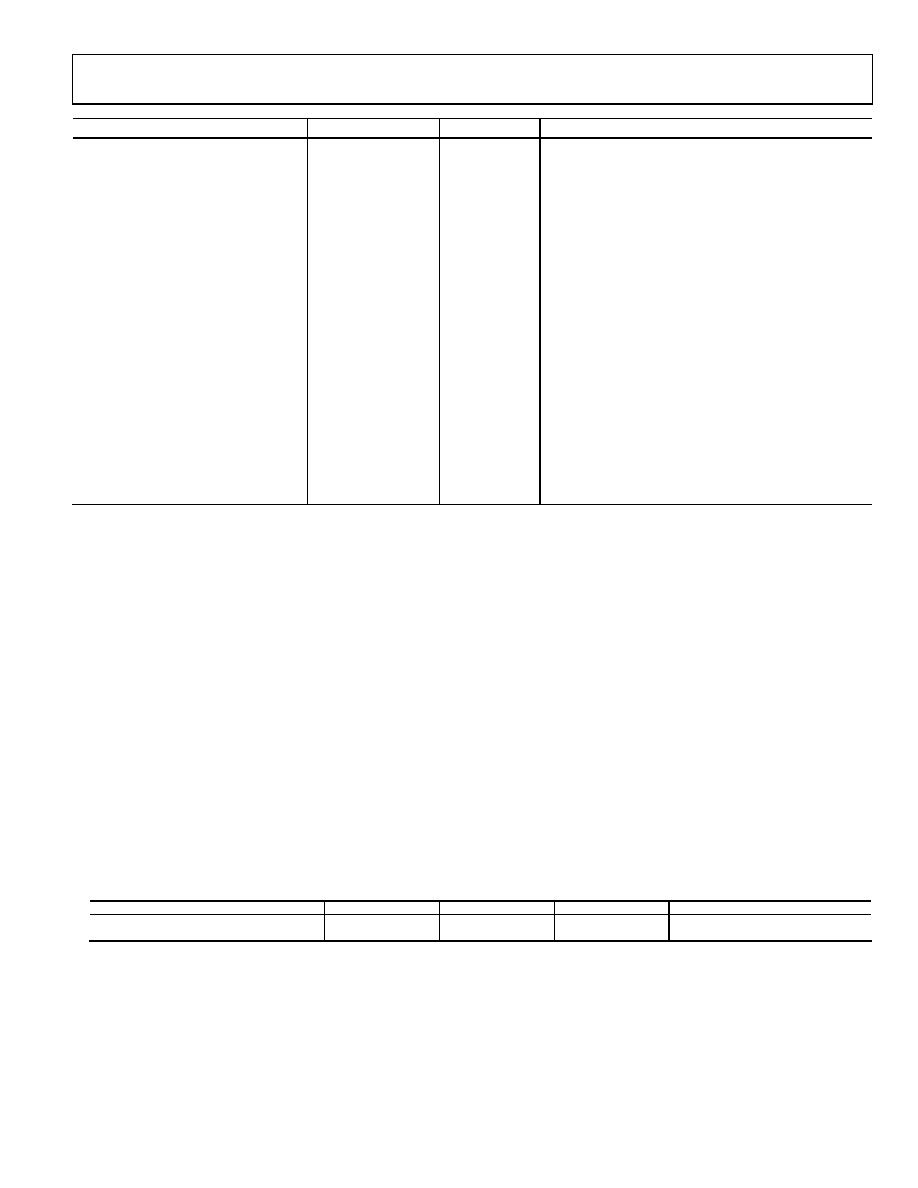
Parameter
B Version1
Unit
Conditions/Comments
POWER REQUIREMENTS
VDD Voltage
2.7 to 3.3
V min to V max
For specified performance
Power Supply Currents17
Digital I/Ps = 0 V or VDD, external MCLK IN and CLKDIS = 1
0.32
mA max
BUF bit = 0, fCLKIN = 1 MHz, gains of 1 to 128
0.6
mA max
BUF bit = 1, fCLKIN = 1 MHz, gains of 1 to 128
0.4
mA max
BUF bit = 0, fCLKIN = 2.4576 MHz, gains of 1 to 4
0.6
mA max
BUF bit = 0, fCLKIN = 2.4576 MHz, gains of 8 to 128
0.7
mA max
BUF bit = 1, fCLKIN = 2.4576 MHz, gains of 1 to 4
1.1
mA max
BUF bit = 1, fCLKIN = 2.4576 MHz, gains of 8 to 128
VDD Voltage
4.75 to 5.25
V min to V max
For specified performance
Power Supply Currents17
Digital I/Ps = 0 V or VDD, external MCLK IN and CLKDIS = 1
0.45
mA max
BUF bit = 0, fCLKIN = 1 MHz, gains of 1 to 128
0.7
mA max
BUF bit = 1, fCLKIN = 1 MHz, gains of 1 to 128
0.6
mA max
BUF bit = 0, fCLKIN = 2.4576 MHz, gains of 1 to 4
0.85
mA max
BUF bit = 0, fCLKIN = 2.4576 MHz, gains of 8 to 128
0.9
mA max
BUF bit = 1, fCLKIN = 2.4576 MHz, gains of 1 to 4
1.3
mA max
BUF bit = 1, fCLKIN = 2.4576 MHz, gains of 8 to 128
Standby (Power-Down) Current18
16
μA max
8
μA max
External MCLK IN = 0 V or VDD, VDD = 3 V
Power Supply Rejection19, 20
dB typ
1 Temperature range is 40°C to +85°C.
2 These numbers are established from characterization or design data at initial product release.
3 A calibration is effectively a conversion; therefore, these errors are of the order of the conversion noise shown in Table 5 and Table 7. This applies after calibration at
the temperature of interest.
4 Recalibration at any temperature removes these drift errors.
5 Positive full-scale error includes zero-scale errors (unipolar offset error or bipolar zero error) and applies to both unipolar and bipolar input ranges.
6 Full-scale drift includes zero-scale drift (unipolar offset drift or bipolar zero drift) and applies to both unipolar and bipolar input ranges.
7 Gain error does not include zero-scale errors. It is calculated as (full-scale error – unipolar offset error) for unipolar ranges and (full-scale error - bipolar zero error) for
bipolar ranges.
8 Gain drift does not include unipolar offset drift or bipolar zero drift. It is effectively the drift of the part if only zero-scale calibrations are performed.
9 This common-mode voltage range is allowed, provided that the input voltage on analog inputs is not more positive than VDD + 30 mV or more negative than
GND 100 mV. Parts are functional with voltages down to GND 200 mV, but with increased leakage at high temperatures.
10 The AD7705/AD7706 can tolerate absolute analog input voltages down to GND 200 mV, but the leakage current increases.
11 The analog input voltage range on AIN(+) is given with respect to the voltage on AIN() on the AD7705, and with respect to the voltage of the COMMON input on the
AD7706. The absolute voltage on the analog inputs should not be more positive than VDD + 30 mV, or more negative than GND 100 mV for specified performance.
Input voltages of GND 200 mV can be accommodated, but with increased leakage at high temperatures.
12 VREF = REFIN(+) REFIN().
13 These logic output levels apply to the MCLK OUT only when it is loaded with one CMOS load.
14 Sample tested at 25°C to ensure compliance.
15 After calibration, if the analog input exceeds positive full scale, the converter outputs all 1s. If the analog input is less than negative full scale, the device outputs all 0s.
16 These calibration and span limits apply, provided that the absolute voltage on the analog inputs does not exceed VDD + 30 mV or go more negative than
GND
100 mV. The offset calibration limit applies to both the unipolar zero point and the bipolar zero point.
17 When using a crystal or ceramic resonator across the MCLK pins as the clock source for the device, the VDD current and power dissipation varies depending on the
crystal or resonator type (see Clocking and Oscillator Circuit section).
18 If the external master clock continues to run in standby mode, the standby current increases to 150 μA typical at 5 V and 75 μA at 3 V. When using a crystal or ceramic
resonator across the MCLK pins as the clock source for the device, the internal oscillator continues to run in standby mode, and the power dissipation depends on the
crystal or resonator type (see Standby Mode section).
19 Measured at dc and applies in the selected pass band. PSRR at 50 Hz exceeds 120 dB, with filter notches of 25 Hz or 50 Hz. PSRR at 60 Hz exceeds 120 dB, with filter
notches of 20 Hz or 60 Hz.
20 PSRR depends on both gain and VDD, as follows:
Gain
1
2
4
8 to 128
VDD = 3 V
86
78
85
93
VDD = 5 V
90
78
84
91
相关PDF资料 |
PDF描述 |
|---|---|
| MS27467T15F18PA | CONN PLUG 18POS STRAIGHT W/PINS |
| D38999/20JG75BN | CONN HSG RCPT 4POS WALL MT SCKT |
| D38999/26MB99SNLC | CONN HSG PLUG 7POS STRGHT SCKT |
| AD7888BR-REEL7 | IC ADC 12BIT 8CHAN SRL 16SOIC |
| D38999/26WG11AB | CONN HSG PLUG 11POS STRGHT PINS |
相关代理商/技术参数 |
参数描述 |
|---|---|
| AD7705BRZ-REEL71 | 制造商:AD 制造商全称:Analog Devices 功能描述:3 V/5 V, 1 mW, 2-/3-Channel, 16-Bit, Sigma-Delta ADCs |
| AD7705EB | 制造商:AD 制造商全称:Analog Devices 功能描述:3 V/5 V 1 mW 2-/3-Channel 16-Bit Sigma-Delta ADCs(264.12 k) |
| AD7706 | 制造商:AD 制造商全称:Analog Devices 功能描述:3 V/5 V, 1 mW 2-/3-Channel 16-Bit, Sigma-Delta ADCs |
| AD7706BN | 功能描述:IC ADC 16BIT 3CH 16-DIP RoHS:否 类别:集成电路 (IC) >> 数据采集 - 模数转换器 系列:- 产品培训模块:Lead (SnPb) Finish for COTS Obsolescence Mitigation Program 标准包装:2,500 系列:- 位数:12 采样率(每秒):3M 数据接口:- 转换器数目:- 功率耗散(最大):- 电压电源:- 工作温度:- 安装类型:表面贴装 封装/外壳:SOT-23-6 供应商设备封装:SOT-23-6 包装:带卷 (TR) 输入数目和类型:- |
发布紧急采购,3分钟左右您将得到回复。