- 您现在的位置:买卖IC网 > PDF目录10247 > AD7707BR (Analog Devices Inc)IC ADC 16BIT 3CH 20-SOIC PDF资料下载
参数资料
| 型号: | AD7707BR |
| 厂商: | Analog Devices Inc |
| 文件页数: | 17/52页 |
| 文件大小: | 0K |
| 描述: | IC ADC 16BIT 3CH 20-SOIC |
| 标准包装: | 37 |
| 位数: | 16 |
| 采样率(每秒): | 500 |
| 数据接口: | DSP,MICROWIRE?,QSPI?,串行,SPI? |
| 转换器数目: | 1 |
| 功率耗散(最大): | 1mW |
| 电压电源: | 模拟和数字 |
| 工作温度: | -40°C ~ 85°C |
| 安装类型: | 表面贴装 |
| 封装/外壳: | 20-SOIC(0.295",7.50mm 宽) |
| 供应商设备封装: | 20-SOIC W |
| 包装: | 管件 |
| 输入数目和类型: | 1 个单端,单极;1 个单端,双极;2 个伪差分,单极;2 个伪差分,双极 |
第1页第2页第3页第4页第5页第6页第7页第8页第9页第10页第11页第12页第13页第14页第15页第16页当前第17页第18页第19页第20页第21页第22页第23页第24页第25页第26页第27页第28页第29页第30页第31页第32页第33页第34页第35页第36页第37页第38页第39页第40页第41页第42页第43页第44页第45页第46页第47页第48页第49页第50页第51页第52页
AD7707
Rev. B | Page 24 of 52
CIRCUIT DESCRIPTION
The AD7707 is a Σ-Δ ADC with on-chip digital filtering, intended
for the measurement of wide dynamic range, low frequency
signals such as those in industrial control or process control
applications. It contains a Σ-Δ (or charge balancing) ADC, a
calibration microcontroller with on-chip static RAM, a clock
oscillator, a digital filter, and a bidirectional serial communica-
tions port. The part consumes only 320 μA of power supply
current, making it ideal for battery-powered or loop-powered
instruments. On-chip thin-film resistors allow ±10 V, ±5 V, 0 V
to 10 V, and 0 V to 5 V high level input signals to be directly
accommodated on the analog input without requiring split
supplies, dc-to-dc converters, or charge pumps. This part operates
with a supply voltage of 2.7 V to 3.3 V, or 4.75 V to 5.25 V.
The AD7707 contains two low level (AIN1 and AIN2) pro-
grammable-gain pseudo differential analog input channels and
one high level (AIN3) single-ended input channel. For the low
level input channels, the selectable gains are 1, 2, 4, 8, 16, 32, 64,
and 128, allowing the part to accept unipolar signals of between
0 mV to 20 mV and 0 V to 2.5 V, or bipolar signals in the range
from ±20 mV to ±2.5 V when the reference input voltage equals
2.5 V. With a reference voltage of 1.225 V, the input ranges are
from 0 mV to 10 mV to 0 V to 1.225 V in unipolar mode, and
from ±10 mV to ±1.225 V in bipolar mode. Note that the signals
are with respect to the LOCOM input.
The high level input channel can directly accept input signals
of ±10 V with respect to HICOM when operating with 5 V
supplies and a reference of 2.5 V. With 3 V supplies, ±5 V can
be accommodated on the AIN3 input.
The input signal to the analog input is continuously sampled at
a rate determined by the frequency of the master clock, MCLK
IN, and the selected gain. A charge-balancing ADC (Σ-Δ
modulator) converts the sampled signal into a digital pulse
train whose duty cycle contains the digital information. The
programmable gain function on the analog input is also
incorporated in this Σ-Δ modulator with the input sampling
frequency being modified to give the higher gains. A sinc3
digital low-pass filter processes the output of the Σ-Δ modulator
and updates the output register at a rate determined by the first
notch frequency of this filter. The output data can be read from
the serial port randomly or periodically at any rate up to the
output register update rate. The first notch of this digital filter
(and therefore its 3 dB frequency) can be programmed via the
clock register bits, FS0 to FS2. With a master clock frequency
of 2.4576 MHz, the programmable range for this first notch
frequency is from 10 Hz to 500 Hz, giving a programmable range
for the 3 dB frequency of 2.62 Hz to 131 Hz. With a master clock
frequency of 1 MHz, the programmable range for this first notch
frequency is from 4 Hz to 200 Hz, giving a programmable range for
the 3 dB frequency of 1.06 Hz to 52.4 Hz.
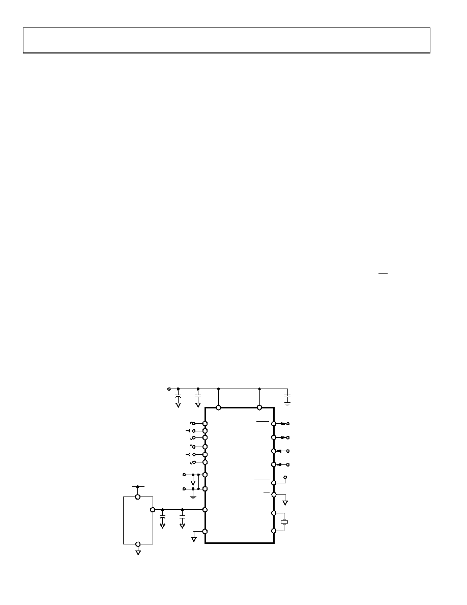
The basic connection diagram for the AD7707 is shown in
provides the reference source for the part. On the digital side,
the part is configured for 3-wire operation with CS tied to
DGND. A quartz crystal or ceramic resonator provides the master
clock source for the part. In most cases, it is necessary to
connect capacitors on the crystal or resonator to ensure that it
does not oscillate at overtones of its fundamental operating
frequency. The values of capacitors can vary, depending on the
manufacturer’s specifications. A similar circuit is applicable for
operation with 3 V supplies; in this case, a 1.225 V reference
(AD1580) should be used for specified performance.
AVDD
DVDD
ANALOG
5V SUPPLY
10F
AIN1
AIN2
LOCOM
AIN3
VBIAS
HICOM
LOW LEVEL
ANALOG
INPUT
HIGH LEVEL
ANALOG
INPUT
AGND
DGND
REF IN(+)
REF IN(–)
10F
VIN
ANALOG 5V
SUPPLY
AD780/
REF192
VOUT
GND
AD7707
DRDY
DATA READY
DOUT
RECEIVE (READ)
DIN
SERIAL DATA
SCLK
SERIAL CLOCK
RESET
5V
CS
MCLK IN
MCLK OUT
CRYSTAL OR
CERAMIC
RESONATOR
0.1F
08
69
1-
0
1
2
Figure 12. Basic Connection Diagram for 5 V Operation
相关PDF资料 |
PDF描述 |
|---|---|
| VE-23Y-MV-F4 | CONVERTER MOD DC/DC 3.3V 99W |
| VE-23J-CU-F1 | CONVERTER MOD DC/DC 36V 200W |
| AD7575JRZ | IC ADC 8BIT LC2MOS W/HOLD 18SOIC |
| VE-23Y-MV-F3 | CONVERTER MOD DC/DC 3.3V 99W |
| VE-23H-CU-F4 | CONVERTER MOD DC/DC 52V 200W |
相关代理商/技术参数 |
参数描述 |
|---|---|
| AD7707BR-REEL | 制造商:Analog Devices 功能描述:ADC Single Delta-Sigma 500sps 16-bit Serial 20-Pin SOIC W T/R 制造商:Analog Devices 功能描述:ADC SGL DELTA-SIGMA 0.5KSPS 16BIT SERL 20SOIC W - Tape and Reel |
| AD7707BR-REEL7 | 制造商:Analog Devices 功能描述:ADC Single Delta-Sigma 500sps 16-bit Serial 20-Pin SOIC W T/R 制造商:Analog Devices 功能描述:ADC SGL DELTA-SIGMA 0.5KSPS 16BIT SERL 20SOIC W - Tape and Reel |
| AD7707BRU | 功能描述:IC ADC 16BIT 3CH 20-TSSOP RoHS:否 类别:集成电路 (IC) >> 数据采集 - 模数转换器 系列:- 标准包装:1,000 系列:- 位数:12 采样率(每秒):300k 数据接口:并联 转换器数目:1 功率耗散(最大):75mW 电压电源:单电源 工作温度:0°C ~ 70°C 安装类型:表面贴装 封装/外壳:24-SOIC(0.295",7.50mm 宽) 供应商设备封装:24-SOIC 包装:带卷 (TR) 输入数目和类型:1 个单端,单极;1 个单端,双极 |
| AD7707BRU-REEL | 制造商:Analog Devices 功能描述:ADC Single Delta-Sigma 500sps 16-bit Serial 20-Pin TSSOP T/R 制造商:Analog Devices 功能描述:ADC SGL DELTA-SIGMA 0.5KSPS 16BIT SERL 20TSSOP - Tape and Reel |
| AD7707BRU-REEL7 | 功能描述:IC ADC 16BIT 3CH 20-TSSOP T/R RoHS:否 类别:集成电路 (IC) >> 数据采集 - 模数转换器 系列:- 标准包装:1,000 系列:- 位数:16 采样率(每秒):45k 数据接口:串行 转换器数目:2 功率耗散(最大):315mW 电压电源:模拟和数字 工作温度:0°C ~ 70°C 安装类型:表面贴装 封装/外壳:28-SOIC(0.295",7.50mm 宽) 供应商设备封装:28-SOIC W 包装:带卷 (TR) 输入数目和类型:2 个单端,单极 |
发布紧急采购,3分钟左右您将得到回复。