- 您现在的位置:买卖IC网 > PDF目录10247 > AD7707BR (Analog Devices Inc)IC ADC 16BIT 3CH 20-SOIC PDF资料下载
参数资料
| 型号: | AD7707BR |
| 厂商: | Analog Devices Inc |
| 文件页数: | 6/52页 |
| 文件大小: | 0K |
| 描述: | IC ADC 16BIT 3CH 20-SOIC |
| 标准包装: | 37 |
| 位数: | 16 |
| 采样率(每秒): | 500 |
| 数据接口: | DSP,MICROWIRE?,QSPI?,串行,SPI? |
| 转换器数目: | 1 |
| 功率耗散(最大): | 1mW |
| 电压电源: | 模拟和数字 |
| 工作温度: | -40°C ~ 85°C |
| 安装类型: | 表面贴装 |
| 封装/外壳: | 20-SOIC(0.295",7.50mm 宽) |
| 供应商设备封装: | 20-SOIC W |
| 包装: | 管件 |
| 输入数目和类型: | 1 个单端,单极;1 个单端,双极;2 个伪差分,单极;2 个伪差分,双极 |
第1页第2页第3页第4页第5页当前第6页第7页第8页第9页第10页第11页第12页第13页第14页第15页第16页第17页第18页第19页第20页第21页第22页第23页第24页第25页第26页第27页第28页第29页第30页第31页第32页第33页第34页第35页第36页第37页第38页第39页第40页第41页第42页第43页第44页第45页第46页第47页第48页第49页第50页第51页第52页
AD7707
Rev. B | Page 14 of 52
OUTPUT NOISE
OUTPUT NOISE FOR LOW LEVEL INPUT
CHANNELS (5 V OPERATION)
Table 7 shows the AD7707 output rms noise and peak-to-peak
resolution in unbuffered mode for the selectable notch and
3 dB frequencies for the part, as selected by FS0, FS1, and FS2
of the clock register. The numbers given are for the bipolar
input ranges with a VREF of 2.5 V and AVDD = 5 V. These
numbers are typical and are generated at an analog input voltage of
0 V. Table 8 shows the rms noise and peak-to-peak resolution
when operating in buffered mode. It is important to note that
the peak-to-peak numbers represent the resolution for which
there is no code flicker. They are not calculated based on rms
noise but on peak-to-peak noise. The numbers given are for
bipolar input ranges with a VREF of 2.5 V. These numbers are
typical and are rounded to the nearest LSB. The numbers apply
for the CLKDIV bit of the clock register set to 0. The output
noise comes from two sources. The first is the electrical noise in
the semiconductor devices (device noise) used in the
implementation of the modulator. Secondly, when the analog
input is converted into the digital domain, quantization noise is
added. The device noise is at a low level and is independent of
frequency. The quantization noise starts at an even lower level
but rises rapidly with increasing frequency to become the
given for the bipolar input ranges. For the unipolar ranges, the
rms noise numbers are the same as the bipolar range but the
peak-to-peak resolution is now based on half the signal range,
which effectively means losing one bit of resolution.
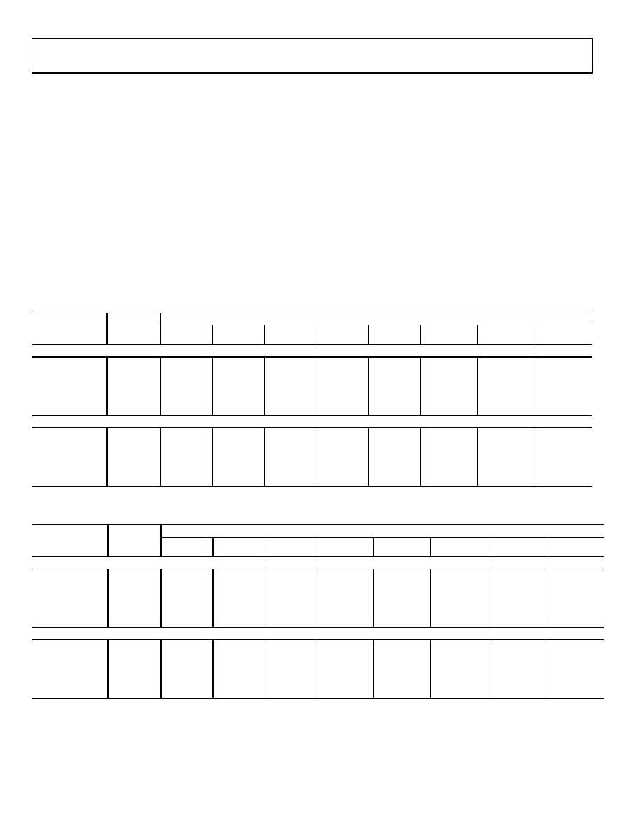
Table 7. Output RMS Noise/Peak-to-Peak Resolution vs. Gain and Output Update Rate @ 5 V AIN1 and AIN2 Unbuffered Mode Only
Filter First Notch
and Output Data
Rate
3 dB
Frequency
Typical Output RMS Noise in μV (Peak-to-Peak Resolution in Bits)
Gain of 1
Gain of 2
Gain of 4
Gain of 8
Gain of 16
Gain of 32
Gain of 64
Gain of 128
MCLK IN = 2.4576 MHz
10 Hz
2.62 Hz
1.2 (16)
0.7 (16)
0.54 (16)
0.28 (16)
0.28 (15.5)
0.27 (14.5)
50 Hz
13.1 Hz
3.6 (16)
2.1 (16)
1.25 (16)
0.89 (16)
0.62 (16)
0.60 (15.5)
0.56 (14.5)
0.56 (13.5)
60 Hz
15.72 Hz
4.7 (16)
2.6 (16)
1.5 (16)
0.94 (16)
0.73 (16)
0.68 (15.5)
0.66 (14.5)
0.63 (13.5)
250 Hz
65.5 Hz
95 (13)
65 (13)
23.4 (13)
11.6 (13)
6.5 (13)
3.4 (13)
2.1 (12.5)
1.5 (12)
500 Hz
131 Hz
600 (10.5)
316 (10.5)
138 (10.5)
71 (10.5)
38 (10.5)
18 (10.5)
10 (10)
5.7 (10)
MCLK IN = 1 MHz
4.05 Hz
1.06 Hz
1.19 (16)
0.69 (16)
0.71 (16)
0.63 (16)
0.27 (16)
0.26 (15.5)
0.24 (15)
20 Hz
5.24 Hz
3.68 (16)
2.18 (16)
1.19 (16)
0.94 (16)
0.6 (16)
0.6 (15.5)
0.56 (14.5)
0.56 (13.5)
25 Hz
6.55 Hz
4.78 (16)
2.66 (16)
1.51 (16)
1.07 (16)
0.7 (16)
0.67 (15.5)
0.66 (14.5)
0.65 (13.5)
100 Hz
26.2 Hz
100 (13)
50.1 (13)
23.5 (13)
11.9 (13)
5.83 (13)
3.64 (13)
2.16 (12.5)
1.5 (12)
200 Hz
52.5 Hz
543 (10.5)
318 (10.5)
132 (10.5)
68.1 (10.5)
33.1 (10.5)
17.6 (10.5)
9.26 (10.5)
6.13 (10)
Table 8. Output RMS Noise/Peak-to-Peak Resolution vs. Gain and Output Update Rate @ 5 V AIN1 and AIN2 Buffered Mode Only
Filter First Notch
and Output Data
Rate
3 dB
Frequency
Typical Output RMS oise in μV (Peak-to-Peak Resolution in Bits)
Gain of 1
Gain of 2
Gain of 4
Gain of 8
Gain of 16
Gain of 32
Gain of 64
Gain of 128
MCLK IN = 2.4576 MHz
10 Hz
2.62 Hz
1.47 (16)
0.95 (16)
0.88 (16)
0.55 (16)
0.42 (16)
0.42 (15)
0.41 (14)
50 Hz
13.1 Hz
4.2 (16)
2.6 (16)
1.6 (16)
1 (16)
0.89 (15.5)
0.94 (15)
0.9 (14)
0.9 (13)
60 Hz
15.72 Hz
4.9 (16)
3 (16)
1.8 (16)
1.1 (16)
1 (15.5)
1 (14.5)
0.94 (14)
0.94 (13)
250 Hz
65.5 Hz
104 (13)
52 (13)
26 (13)
14 (13)
6.5 (13)
4.1 (12.5)
2.7 (12.5)
2.3 (11.5)
500 Hz
131 Hz
572 (10.5)
293 (10.5)
125 (10.5)
69 (10.5)
40 (10.5)
19 (10.5)
10 (10.5)
5.9 (10)
MCLK IN = 1 MHz
4.05 Hz
1.06 Hz
1.48 (16)
8.95 (16)
0.87 (16)
0.67 (16)
0.41 (16)
0.40 (16)
0.40 (15)
0.40 (14)
20 Hz
5.24 Hz
3.9 (16)
2.46 (16)
1.77 (16)
1.19 (16)
0.94 (16)
0.93 (15)
0.95 (14)
0.9 (13)
25 Hz
6.55 Hz
5.37 (16)
3.05 (16)
1.89 (16)
1.33 (16)
1.11 (15.5)
1.06 (14.5)
1.04 (13.5)
1.02 (12.5)
100 Hz
26.2 Hz
98.9 (13)
52.4 (13)
26.1 (13)
12.7 (13)
6.08 (13)
4.01 (12.5)
2.62 (12.5)
2.33 (11.5)
200 Hz
52.4 Hz
596 (10.5)
298 (10.5)
133 (10.5)
69.3 (10.5)
34.7 (10.5)
16.9 (10.5)
9.67 (10.5)
6.34 (10)
相关PDF资料 |
PDF描述 |
|---|---|
| VE-23Y-MV-F4 | CONVERTER MOD DC/DC 3.3V 99W |
| VE-23J-CU-F1 | CONVERTER MOD DC/DC 36V 200W |
| AD7575JRZ | IC ADC 8BIT LC2MOS W/HOLD 18SOIC |
| VE-23Y-MV-F3 | CONVERTER MOD DC/DC 3.3V 99W |
| VE-23H-CU-F4 | CONVERTER MOD DC/DC 52V 200W |
相关代理商/技术参数 |
参数描述 |
|---|---|
| AD7707BR-REEL | 制造商:Analog Devices 功能描述:ADC Single Delta-Sigma 500sps 16-bit Serial 20-Pin SOIC W T/R 制造商:Analog Devices 功能描述:ADC SGL DELTA-SIGMA 0.5KSPS 16BIT SERL 20SOIC W - Tape and Reel |
| AD7707BR-REEL7 | 制造商:Analog Devices 功能描述:ADC Single Delta-Sigma 500sps 16-bit Serial 20-Pin SOIC W T/R 制造商:Analog Devices 功能描述:ADC SGL DELTA-SIGMA 0.5KSPS 16BIT SERL 20SOIC W - Tape and Reel |
| AD7707BRU | 功能描述:IC ADC 16BIT 3CH 20-TSSOP RoHS:否 类别:集成电路 (IC) >> 数据采集 - 模数转换器 系列:- 标准包装:1,000 系列:- 位数:12 采样率(每秒):300k 数据接口:并联 转换器数目:1 功率耗散(最大):75mW 电压电源:单电源 工作温度:0°C ~ 70°C 安装类型:表面贴装 封装/外壳:24-SOIC(0.295",7.50mm 宽) 供应商设备封装:24-SOIC 包装:带卷 (TR) 输入数目和类型:1 个单端,单极;1 个单端,双极 |
| AD7707BRU-REEL | 制造商:Analog Devices 功能描述:ADC Single Delta-Sigma 500sps 16-bit Serial 20-Pin TSSOP T/R 制造商:Analog Devices 功能描述:ADC SGL DELTA-SIGMA 0.5KSPS 16BIT SERL 20TSSOP - Tape and Reel |
| AD7707BRU-REEL7 | 功能描述:IC ADC 16BIT 3CH 20-TSSOP T/R RoHS:否 类别:集成电路 (IC) >> 数据采集 - 模数转换器 系列:- 标准包装:1,000 系列:- 位数:16 采样率(每秒):45k 数据接口:串行 转换器数目:2 功率耗散(最大):315mW 电压电源:模拟和数字 工作温度:0°C ~ 70°C 安装类型:表面贴装 封装/外壳:28-SOIC(0.295",7.50mm 宽) 供应商设备封装:28-SOIC W 包装:带卷 (TR) 输入数目和类型:2 个单端,单极 |
发布紧急采购,3分钟左右您将得到回复。