- 您现在的位置:买卖IC网 > PDF目录10253 > AD7708BRU (Analog Devices Inc)IC ADC 16BIT R-R 8/10CH 28-TSSOP PDF资料下载
参数资料
| 型号: | AD7708BRU |
| 厂商: | Analog Devices Inc |
| 文件页数: | 32/44页 |
| 文件大小: | 0K |
| 描述: | IC ADC 16BIT R-R 8/10CH 28-TSSOP |
| 标准包装: | 50 |
| 位数: | 16 |
| 采样率(每秒): | 1.37k |
| 数据接口: | DSP,MICROWIRE?,QSPI?,串行,SPI? |
| 转换器数目: | 1 |
| 功率耗散(最大): | 3.84mW |
| 电压电源: | 模拟和数字 |
| 工作温度: | -40°C ~ 85°C |
| 安装类型: | 表面贴装 |
| 封装/外壳: | 28-TSSOP(0.173",4.40mm 宽) |
| 供应商设备封装: | 28-TSSOP |
| 包装: | 管件 |
| 输入数目和类型: | 4 个差分,单极;4 个差分,双极;8 个伪差分,单极;8 个伪差分,双极 |
| 配用: | EVAL-AD7708EBZ-ND - BOARD EVAL FOR AD7708 |
第1页第2页第3页第4页第5页第6页第7页第8页第9页第10页第11页第12页第13页第14页第15页第16页第17页第18页第19页第20页第21页第22页第23页第24页第25页第26页第27页第28页第29页第30页第31页当前第32页第33页第34页第35页第36页第37页第38页第39页第40页第41页第42页第43页第44页
REV. 0
–38–
AD7708/AD7718
Nonchop Mode of Operation (
CHOP = 1)
Chopping is enabled and disabled using the
CHOP bit in the
mode register. Chopping is disabled by loading a 1 to the chop
bit in the mode register. With chopping disabled the available
output rates vary from 16.06 Hz (62.26 ms) to 1365.33 Hz (0.73 ms).
The range of applicable SF words is from 3 to 255. When the
chopping is disabled the channel output data rate is increased by a
factor of 3 compared to the situation when chopping is enabled
and using the same SF word. When used in multiplexed
applications, operation with chop disabled will offer the best
throughput time when cycling through all channels. The drawback
with chop disabled is that the drift performance is degraded
and calibration is required following a gain change or significant
temperature change. The output update and filter decimation
rate is again controlled by the SF word loaded to the filter
register. The digital filter frequency response places sinc
3
notches at integer multiples of the update rate. The output
update rate f
f
SF
ADC
MOD
=
×
8
. The AD7708/AD7718 are targeted
at multiplexed applications and therefore operating with chop
disabled optimizes channel throughput time. One of the key
requirements in these applications is the selection of an SF word
so as to obtain the maximum filter rejection at 50 Hz and 60 Hz
while minimizing the channel throughput rate. This is achieved
with an SF word of 75 giving 57 dB rejection at 50 Hz, and
60 dB rejection at 60 Hz while offering a channel throughput
time of 55 ms. Using a higher SF word of 151, 50 Hz and
60 Hz rejection can be maximized at 60 dB with a channel
throughput rate of 110 ms. An SF word of 255 gives maximum
rejection at both 50 Hz and 60 Hz but the channel throughput
rate is restricted to 186 ms. Table XXI shows a quick comparison
of normal mode 50 Hz and 60 Hz rejection, settling time, and
update rate for a selection of SF words with chop both enabled
and disabled.
Programmable Gain Amplifier
The output from the buffer is applied to the input of the program-
mable gain amplifier (PGA). The PGA gain range is programmed
via the range bits in the ADCCON register. The PGA has eight
ranges. With an external 2.5 V reference applied, and a PGA
setting of 128, the unipolar analog input range is 0 mV to 20 mV,
while the bipolar analog input range is
±20 mV. With a PGA
setting of 1, the unipolar and bipolar input ranges are 2.56 V.
When operating with chop mode enabled (
CHOP = 0), the ADC
range-matching specification of 2
V (typ) across all ranges
means that calibration need only be carried out on a single
range and does not have to be repeated when the PGA range is
changed. This is a significant advantage when compared with
similar ADCs available on the market. Typical matching across
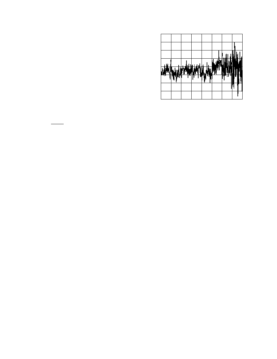
ranges is shown in Figure 25. Here, the ADC is configured in
fully-differential, bipolar mode with an external 2.5 V reference,
while an analog input voltage of just greater than 19 mV is forced
on its analog inputs. The ADC continuously converts the dc
voltage at an update rate of 5.35 Hz, i.e., SF = FFhex, 800
conversion results in total are gathered. The first 100 results are
gathered with the ADC operating with a PGA setting of 128.
19.367
100
0
200
400
300
19.371
19.370
19.369
19.368
19.372
ADC
INPUT
V
O
L
T
A
GE
–
mV
500
19.366
19.365
19.364
600
700
800
SAMPLE COUNT
ADC RANGE
20mV
40mV
80mV
160mV
320mV
640mV
1.28V
2.56V
Figure 25. ADC Range Matching
The PGA setting is then switched to 64 and 100 more results
are gathered, and so on until the last 100 samples are gathered
with a PGA setting of 1. From Figure 25, the variation in the sample
mean through each range, i.e., the range matching, is seen to be
of the order of 2
V. When operating with chop mode disabled
(
CHOP = 1), new calibration data is needed (but not necessarily
a new calibration) to remove offset error when switching channels.
Bipolar/Unipolar Configuration
The analog inputs on the AD7708/AD7718 can accept either
unipolar or bipolar input voltage ranges. Bipolar input ranges
does not imply that the part can handle negative voltages with
respect to system AGND. Signals in pseudo-differential mode
are referenced to AINCOM, while in fully differential mode they
are referenced to the negative input of the differential input. For
example, if AINCOM is 2.5 V and the AD7708/AD7718 AIN1
analog input is configured for an analog input range of 0 mV to
+20 mV, the input voltage range on the AIN1 input is 2.5 V to
2.52 V. If AINCOM is 2.5 V and the AD7708/AD7718 is con-
figured for an analog input range of
±1.28 V, the analog input
range on the AIN1 input is 1.22 V to 3.78 V (i.e., 2.5 V
±
1.28 V). Bipolar or unipolar options are chosen by programming
U/
B bit in the ADCCON register. Programming for either
unipolar or bipolar operation does not change any of the input
signal conditioning; it simply changes the data output coding
and the points on the transfer function where calibrations occur.
Data Output Coding
When the AD7718 is configured for unipolar operation, the out-
put coding is natural (straight) binary with a zero differential
input voltage resulting in a code of 000 . . . 000, a midscale
voltage resulting in a code of 100 . . . 000, and a full-scale input
voltage resulting in a code of 111 . . . 111. The output code for
any analog input voltage can be represented as follows:
Code = (AIN
× GAIN × 224)/(1.024 × VREF)
where
AIN is the analog input voltage,
GAIN is the PGA gain, i.e., 1 on the 2.5 V range and 128 on
the 20 mV range.
相关PDF资料 |
PDF描述 |
|---|---|
| MS3106F20-29PW | CONN PLUG 17POS STRAIGHT W/PINS |
| MS3106F20-29P | CONN PLUG 17POS STRAIGHT W/PINS |
| MS3106E20-29P | CONN PLUG 17POS STRAIGHT W/PINS |
| MS27656E11F4P | CONN RCPT 4POS WALL MNT W/PINS |
| MS27467T15F5PC | CONN PLUG 5POS STRAIGHT W/PINS |
相关代理商/技术参数 |
参数描述 |
|---|---|
| AD7708BRU-REEL | 功能描述:IC ADC 16BIT R-R 8/10CH 28-TSSOP RoHS:否 类别:集成电路 (IC) >> 数据采集 - 模数转换器 系列:- 标准包装:1,000 系列:- 位数:16 采样率(每秒):45k 数据接口:串行 转换器数目:2 功率耗散(最大):315mW 电压电源:模拟和数字 工作温度:0°C ~ 70°C 安装类型:表面贴装 封装/外壳:28-SOIC(0.295",7.50mm 宽) 供应商设备封装:28-SOIC W 包装:带卷 (TR) 输入数目和类型:2 个单端,单极 |
| AD7708BRU-REEL7 | 功能描述:IC ADC 16BIT R-R 8/10CH 28-TSSOP RoHS:否 类别:集成电路 (IC) >> 数据采集 - 模数转换器 系列:- 标准包装:1,000 系列:- 位数:16 采样率(每秒):45k 数据接口:串行 转换器数目:2 功率耗散(最大):315mW 电压电源:模拟和数字 工作温度:0°C ~ 70°C 安装类型:表面贴装 封装/外壳:28-SOIC(0.295",7.50mm 宽) 供应商设备封装:28-SOIC W 包装:带卷 (TR) 输入数目和类型:2 个单端,单极 |
| AD7708BRUZ | 功能描述:IC ADC 16BIT R-R 8/10CH 28-TSSOP RoHS:是 类别:集成电路 (IC) >> 数据采集 - 模数转换器 系列:- 标准包装:1 系列:microPOWER™ 位数:8 采样率(每秒):1M 数据接口:串行,SPI? 转换器数目:1 功率耗散(最大):- 电压电源:模拟和数字 工作温度:-40°C ~ 125°C 安装类型:表面贴装 封装/外壳:24-VFQFN 裸露焊盘 供应商设备封装:24-VQFN 裸露焊盘(4x4) 包装:Digi-Reel® 输入数目和类型:8 个单端,单极 产品目录页面:892 (CN2011-ZH PDF) 其它名称:296-25851-6 |
| AD7708BRUZ-REEL | 功能描述:IC ADC 16BIT R-R 8/10CH 28TSSOP RoHS:是 类别:集成电路 (IC) >> 数据采集 - 模数转换器 系列:- 标准包装:1,000 系列:- 位数:16 采样率(每秒):45k 数据接口:串行 转换器数目:2 功率耗散(最大):315mW 电压电源:模拟和数字 工作温度:0°C ~ 70°C 安装类型:表面贴装 封装/外壳:28-SOIC(0.295",7.50mm 宽) 供应商设备封装:28-SOIC W 包装:带卷 (TR) 输入数目和类型:2 个单端,单极 |
| AD7708BRUZ-REEL7 | 功能描述:IC ADC 16BIT R-R 8/10CH 28TSSOP RoHS:是 类别:集成电路 (IC) >> 数据采集 - 模数转换器 系列:- 标准包装:1,000 系列:- 位数:16 采样率(每秒):45k 数据接口:串行 转换器数目:2 功率耗散(最大):315mW 电压电源:模拟和数字 工作温度:0°C ~ 70°C 安装类型:表面贴装 封装/外壳:28-SOIC(0.295",7.50mm 宽) 供应商设备封装:28-SOIC W 包装:带卷 (TR) 输入数目和类型:2 个单端,单极 |
发布紧急采购,3分钟左右您将得到回复。