- 您现在的位置:买卖IC网 > PDF目录10253 > AD7708BRU (Analog Devices Inc)IC ADC 16BIT R-R 8/10CH 28-TSSOP PDF资料下载
参数资料
| 型号: | AD7708BRU |
| 厂商: | Analog Devices Inc |
| 文件页数: | 36/44页 |
| 文件大小: | 0K |
| 描述: | IC ADC 16BIT R-R 8/10CH 28-TSSOP |
| 标准包装: | 50 |
| 位数: | 16 |
| 采样率(每秒): | 1.37k |
| 数据接口: | DSP,MICROWIRE?,QSPI?,串行,SPI? |
| 转换器数目: | 1 |
| 功率耗散(最大): | 3.84mW |
| 电压电源: | 模拟和数字 |
| 工作温度: | -40°C ~ 85°C |
| 安装类型: | 表面贴装 |
| 封装/外壳: | 28-TSSOP(0.173",4.40mm 宽) |
| 供应商设备封装: | 28-TSSOP |
| 包装: | 管件 |
| 输入数目和类型: | 4 个差分,单极;4 个差分,双极;8 个伪差分,单极;8 个伪差分,双极 |
| 配用: | EVAL-AD7708EBZ-ND - BOARD EVAL FOR AD7708 |
第1页第2页第3页第4页第5页第6页第7页第8页第9页第10页第11页第12页第13页第14页第15页第16页第17页第18页第19页第20页第21页第22页第23页第24页第25页第26页第27页第28页第29页第30页第31页第32页第33页第34页第35页当前第36页第37页第38页第39页第40页第41页第42页第43页第44页
REV. 0
AD7708/AD7718
–41–
Good decoupling is important when using high resolution ADCs.
All analog supplies should be decoupled with 10
F tantalum in
parallel with 0.1
F capacitors to AGND. To achieve the best
from these decoupling components, they have to be placed
as close as possible to the device, ideally right up against the
device. All logic chips should be decoupled with 0.1
F ceramic
capacitors to DGND. In systems where a common supply
voltage is used to drive both the AVDD and DVDD of the AD7708/
AD7718, it is recommended that the system’s AVDD supply is
used. This supply should have the recommended analog supply
decoupling capacitors between the AVDD pin of the AD7708/
AD7718 and AGND and the recommended digital supply
decoupling capacitor between the DVDD pin of the AD7708/
AD7718 and DGND.
APPLICATIONS
The AD7708/AD7718 provides a low cost, high resolution
analog-to-digital function. The AD7708 offers 16-bit resolution
while the AD7718 offers 24-bit resolution. The AD7708 and
AD7718 are pin and function compatible. The AD7718 allows a
direct upgradable path from a 16-bit to a 24-bit system with
minimal software and no hardware changes. Because the analog-
to-digital function is provided by a sigma-delta architecture, it
makes the part more immune to noisy environments, thus mak-
ing the part ideal for use in sensor measurement and in industrial
and process control applications. There are two modes of operation
associated with the AD7708/AD7718, chop enabled (
CHOP = 0)
or chop disabled (
CHOP = 1). With chop enabled the signal chain
is chopped and the device is factory-calibrated at final test in
this mode. Field calibration can be avoided due to the extremely
low offset and gain drifts exhibited by the converter in this
mode. While operating in this mode gives optimum performance
in terms of offset error and offset and gain drift performance, it
offers limited throughput when cycling through all channels.
With chopping disabled, the signal chain is not chopped and
therefore the user needs to ensure that the ADC is calibrated on
range changes and if there is a significant temperature change
as the gain and offset drift performance is degraded.
The key advantage in using the AD7708/AD7718 with chopping
disabled is in channel cycling applications where system through-
put is of prime importance. The max conversion rate with chop
disabled is 1.36 kHz compared with 105 Hz with chop enabled.
The AD7708/AD7718 also provides a programmable gain ampli-
fier, a digital filter, and system calibration options. Thus, it
provides far more system level functionality than off-the-shelf
integrating ADCs without the disadvantage of having to sup-
ply a high quality integrating capacitor. In addition, using the
AD7708/AD7718 in a system allows the system designer to
achieve a much higher level of resolution because noise perfor-
mance of the AD7708/AD7718 is significantly better than that
of integrating ADCs.
The on-chip PGA allows the AD7708/AD7718 to handle an
analog input voltage range as low as 10 mV full scale with VREF
= 1.25 V. The AD7708/AD7718 can be operated in 8-channel
mode with two reference input options or 10-channel mode with
one reference input. Eight-channel mode allows both ratiometric
or absolute measurements to be performed on any channel using
the two reference input options. The differential analog inputs
of the part allow this analog input range to have an absolute
value anywhere between AGND + 100 mV and AVDD – 100 mV.
The buffer on the negative analog input can be bypassed allowing
the AD7708/AD7718 be operated as eight or ten single-ended
input channels. The PGA allows the user to connect transducers
directly to the input of the AD7708/AD7718. The program-
mable gain front end on the AD7708/AD7718 allows the part to
handle unipolar analog input ranges from 0 mV to +20 mV to
0 V to +2.5 V and bipolar inputs of
±20 mV to ±2.5 V. Because
the part operates from a single supply these bipolar ranges are
with respect to a biased-up differential input.
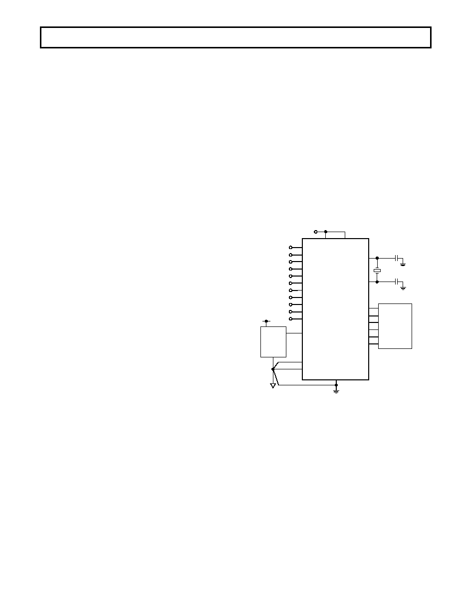
Data Acquisition
The AD7708/AD7718, with its different configuration options
(five fully-differential input or 10 pseudo-differential input
channels with one reference input or four fully-differential input
or eight pseudo-differential input channels with two reference
inputs), is suited to low bandwidth, high resolution data acquisi-
tion systems. In addition, the 3-wire digital interface allows this
data acquisition front end to be isolated with just three opto-
isolators. The entire system can be operated from a single 3 V
or 5 V supply, provided that the input signals to the AD7708/
AD7718’s analog inputs are all of positive polarity.
5V
AD780
AIN6
AIN5
AIN4
AIN3
AIN2
AIN1
5V
GND
VIN
VOUT
AGND
DGND
AVDD
DVDD
REF1IN(–)
MCLKIN
MCLKOUT
32kHz
AD7708/
AD7718
AIN8
AIN7
AIN9
AINCOM
AIN10
MICRO-
CONTROLLER
SCLK
CS
DIN
DOUT
RDY
RESET
REFIN1(+)
Figure 26. Data Acquisition Using the AD7708/AD7718
Programmable Logic Controllers
The AD7708/AD7718 is also suited to programmable logic
controller applications. In such applications, the ADC is required
to handle signals from a variety of different transducers. The
AD7708/AD7718’s programmable gain front end allows the
part to either handle low level signals directly from a transducer
or full-scale signals that have already been conditioned. The faster
throughput rate and settling time of the part when operated with
chopping disabled makes this the optimum mode of operation in
PLC applications as an important feature in these applications is
loop response time. The configuration of the AD7708/AD7718
in PLC applications is similar to that outlined for a data acquisi-
tion system and is shown in Figure 26. In this application the
AD7708/AD7718 is configured in 10-channel mode, (CHCON
= 1) and can be operated as 10 pseudo-differential inputs with
respect to AINCOM or as five fully-differential input channels.
相关PDF资料 |
PDF描述 |
|---|---|
| MS3106F20-29PW | CONN PLUG 17POS STRAIGHT W/PINS |
| MS3106F20-29P | CONN PLUG 17POS STRAIGHT W/PINS |
| MS3106E20-29P | CONN PLUG 17POS STRAIGHT W/PINS |
| MS27656E11F4P | CONN RCPT 4POS WALL MNT W/PINS |
| MS27467T15F5PC | CONN PLUG 5POS STRAIGHT W/PINS |
相关代理商/技术参数 |
参数描述 |
|---|---|
| AD7708BRU-REEL | 功能描述:IC ADC 16BIT R-R 8/10CH 28-TSSOP RoHS:否 类别:集成电路 (IC) >> 数据采集 - 模数转换器 系列:- 标准包装:1,000 系列:- 位数:16 采样率(每秒):45k 数据接口:串行 转换器数目:2 功率耗散(最大):315mW 电压电源:模拟和数字 工作温度:0°C ~ 70°C 安装类型:表面贴装 封装/外壳:28-SOIC(0.295",7.50mm 宽) 供应商设备封装:28-SOIC W 包装:带卷 (TR) 输入数目和类型:2 个单端,单极 |
| AD7708BRU-REEL7 | 功能描述:IC ADC 16BIT R-R 8/10CH 28-TSSOP RoHS:否 类别:集成电路 (IC) >> 数据采集 - 模数转换器 系列:- 标准包装:1,000 系列:- 位数:16 采样率(每秒):45k 数据接口:串行 转换器数目:2 功率耗散(最大):315mW 电压电源:模拟和数字 工作温度:0°C ~ 70°C 安装类型:表面贴装 封装/外壳:28-SOIC(0.295",7.50mm 宽) 供应商设备封装:28-SOIC W 包装:带卷 (TR) 输入数目和类型:2 个单端,单极 |
| AD7708BRUZ | 功能描述:IC ADC 16BIT R-R 8/10CH 28-TSSOP RoHS:是 类别:集成电路 (IC) >> 数据采集 - 模数转换器 系列:- 标准包装:1 系列:microPOWER™ 位数:8 采样率(每秒):1M 数据接口:串行,SPI? 转换器数目:1 功率耗散(最大):- 电压电源:模拟和数字 工作温度:-40°C ~ 125°C 安装类型:表面贴装 封装/外壳:24-VFQFN 裸露焊盘 供应商设备封装:24-VQFN 裸露焊盘(4x4) 包装:Digi-Reel® 输入数目和类型:8 个单端,单极 产品目录页面:892 (CN2011-ZH PDF) 其它名称:296-25851-6 |
| AD7708BRUZ-REEL | 功能描述:IC ADC 16BIT R-R 8/10CH 28TSSOP RoHS:是 类别:集成电路 (IC) >> 数据采集 - 模数转换器 系列:- 标准包装:1,000 系列:- 位数:16 采样率(每秒):45k 数据接口:串行 转换器数目:2 功率耗散(最大):315mW 电压电源:模拟和数字 工作温度:0°C ~ 70°C 安装类型:表面贴装 封装/外壳:28-SOIC(0.295",7.50mm 宽) 供应商设备封装:28-SOIC W 包装:带卷 (TR) 输入数目和类型:2 个单端,单极 |
| AD7708BRUZ-REEL7 | 功能描述:IC ADC 16BIT R-R 8/10CH 28TSSOP RoHS:是 类别:集成电路 (IC) >> 数据采集 - 模数转换器 系列:- 标准包装:1,000 系列:- 位数:16 采样率(每秒):45k 数据接口:串行 转换器数目:2 功率耗散(最大):315mW 电压电源:模拟和数字 工作温度:0°C ~ 70°C 安装类型:表面贴装 封装/外壳:28-SOIC(0.295",7.50mm 宽) 供应商设备封装:28-SOIC W 包装:带卷 (TR) 输入数目和类型:2 个单端,单极 |
发布紧急采购,3分钟左右您将得到回复。