- 您现在的位置:买卖IC网 > PDF目录10252 > AD7709BRU (Analog Devices Inc)IC ADC 16BIT SIGMA-DELTA 24TSSOP PDF资料下载
参数资料
| 型号: | AD7709BRU |
| 厂商: | Analog Devices Inc |
| 文件页数: | 16/32页 |
| 文件大小: | 0K |
| 描述: | IC ADC 16BIT SIGMA-DELTA 24TSSOP |
| 标准包装: | 62 |
| 位数: | 16 |
| 采样率(每秒): | 105 |
| 数据接口: | DSP,MICROWIRE?,QSPI?,串行,SPI? |
| 转换器数目: | 1 |
| 功率耗散(最大): | 3.75mW |
| 电压电源: | 单电源 |
| 工作温度: | -40°C ~ 85°C |
| 安装类型: | 表面贴装 |
| 封装/外壳: | 24-TSSOP(0.173",4.40mm 宽) |
| 供应商设备封装: | 24-TSSOP |
| 包装: | 管件 |
| 输入数目和类型: | 2 个差分,单极;2 个差分,双极;4 个伪差分,单极;4 个伪差分,双极 |
第1页第2页第3页第4页第5页第6页第7页第8页第9页第10页第11页第12页第13页第14页第15页当前第16页第17页第18页第19页第20页第21页第22页第23页第24页第25页第26页第27页第28页第29页第30页第31页第32页
REV. A
AD7709
–23–
Programmable Gain Amplifier
The output from the buffer on the ADC is applied to the input
of the on-chip programmable gain amplifier (PGA). The PGA
can be programmed through eight different unipolar and bipolar
ranges. The PGA gain range is programmed via the range bits
in the Configuration Register. With an external 2.5 V reference
applied, the unipolar ranges are 0 mV to 20 mV, 0 mV to 40 mV,
0 mV to 80 mV, 0 mV to 160 mV, 0 mV to 320 mV, 0 mV to
640 mV, 0 V to 1.28 V, and 0 to 2.56 V, while bipolar ranges
are
±20 mV, ±40 mV, ±80 mV, ±160 mV, ±320 mV, ±640
mV,
±1.28 V, and ±2.56 V. These are the ranges that should
appear at the input to the on-chip PGA.
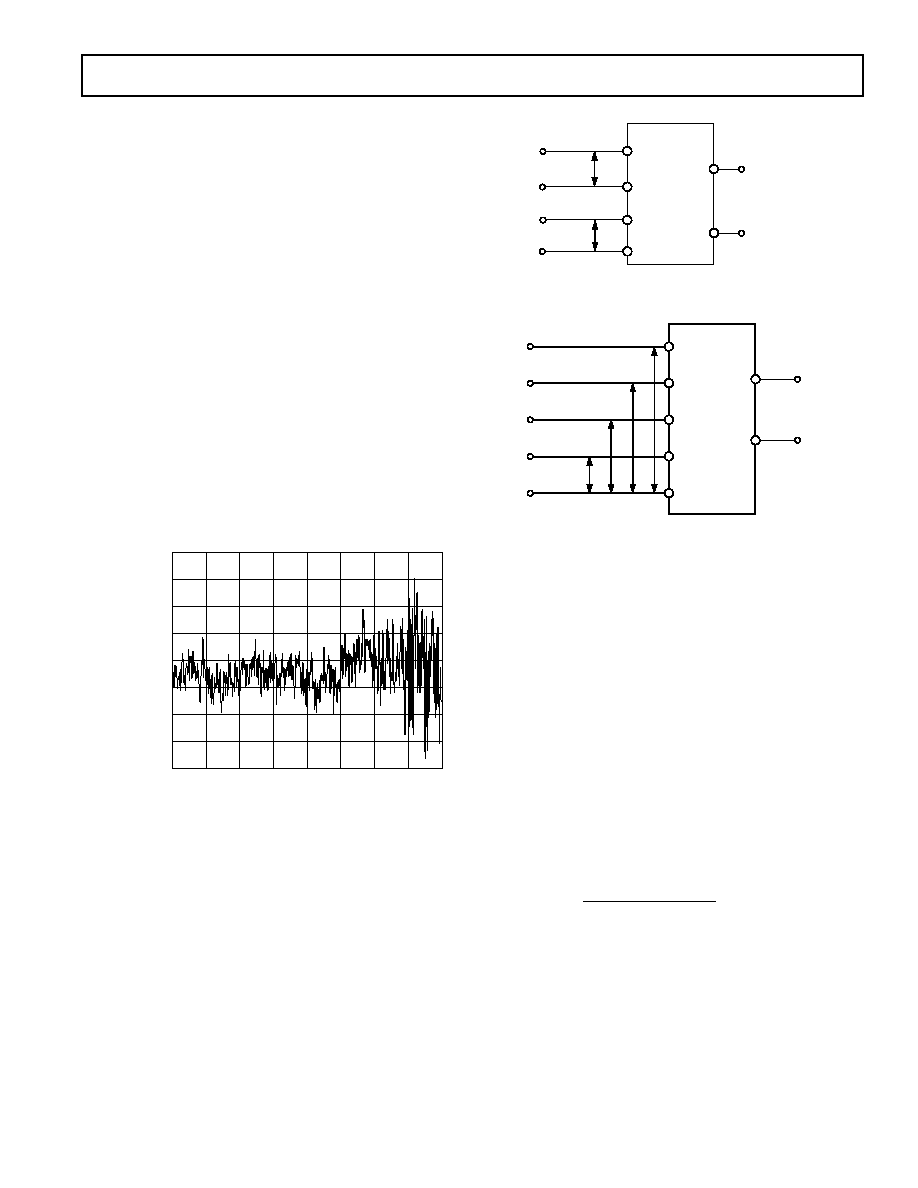
Typical matching across ranges is shown in Figure 15. Here, the
ADC is configured in fully differential, bipolar mode with an
external 2.5 V reference, while an analog input voltage of just
greater than 19 mV is forced on its analog inputs. The ADC
continuously converts the dc voltage at an update rate of 5.35 Hz,
i.e., SF = FFh. A total of 800 conversion results are gathered.
The first 100 results gathered with the ADC operating in the
±20 mV. The ADC range is then switched to ±40 mV and 100
more results are gathered, and so on, until the last 100 samples
are gathered with the ADC configured in the
±2.5 V range. From
Figure 15, the variation in the sample mean through each range,
i.e., the range matching, is seen to be on the order of 2
V.
0
100
200
300
400
500
600
700
800
SAMPLE COUNT
ADC
INPUT
VOLTAGE
–
mV
19.372
19.371
19.370
19.369
19.368
19.367
19.366
19.365
19.364
ADC RANGE
20mV
40mV
80mV
160mV
320mV
640mV
1.28V
2.56V
Figure 15. ADC Range Matching
Bipolar/Unipolar Configuration
The analog inputs on the AD7709 can accept either unipolar or
bipolar input voltage ranges. Bipolar input ranges do not imply that
the part can handle negative voltages with respect to system
GND. Unipolar and bipolar signals on the AIN(+) input on
the ADC are referenced to the voltage on the respective AIN(–)
input. AIN(+) and AIN(–) refer to the signals seen by the
modulator that come from the output of the multiplexer, as shown
in Figures 16 and 17.
FULLY DIFFERENTIAL
AIN(+)
AIN(–)
AIN1
AIN2
AIN3
AIN4
AIN1
AIN2
AIN3
AIN4
MUX
ADC CHANNEL
Figure 16. Fully Differential Mode of Operation
AIN3
AIN4
AIN1/AINCOM
PSEUDO-DIFFERENTIAL
INPUT
AIN(–)
AIN(+)
AIN1
AIN2
AINCOM
ADC CHANNEL
MUX
AIN2/AINCOM
AIN3/AINCOM
AIN4/AINCOM
PSEUDO-DIFFERENTIAL
INPUT
Figure 17. Pseudo-Differential Mode of Operation
For example, if AIN(–) is 2.5 V and the ADC is configured for
an analog input range of 0 mV to 20 mV, the input voltage range
on the AIN(+) input is 2.5 V to 2.52 V. If AIN(–) is 2.5 V and
the AD7709 is configured for an analog input range of
±1.28 V,
the analog input range on the AIN(+) input is 1.22 V to 3.78 V
(i.e., 2.5 V
±1.28 V). Bipolar or unipolar options are chosen by
programming the UNI bit in the Configuration Register. This
programs the ADC for either unipolar or bipolar operation.
Programming for either unipolar or bipolar operation does not
change any of the input signal conditioning; it simply changes
the data output coding.
Data Output Coding
When the ADC is configured for unipolar operation, the output
coding is natural (straight) binary with a zero differential input
voltage resulting in a code of 000 . . . 000, a midscale voltage
resulting in a code of 100 . . . 000, and a full-scale input voltage
resulting in a code of 111 . . . 111. The output code for any analog
input voltage on the ADC can be represented as follows:
Code
AIN
GAIN
V
N
REF
=
××
()
×
()
2
1 024
.
where:
AIN is the analog input voltage.
GAIN is the PGA gain, i.e., 1 on the 2.56 V range and 128 on
the 20 mV range.
N = 16.
相关PDF资料 |
PDF描述 |
|---|---|
| VE-230-MX-F1 | CONVERTER MOD DC/DC 5V 75W |
| LTC2250CUH#TRPBF | IC ADC 10BIT 105MSPS 3V 32-QFN |
| VE-22W-MX-F4 | CONVERTER MOD DC/DC 5.5V 75W |
| VE-22W-MX-F3 | CONVERTER MOD DC/DC 5.5V 75W |
| VE-22W-MX-F2 | CONVERTER MOD DC/DC 5.5V 75W |
相关代理商/技术参数 |
参数描述 |
|---|---|
| AD7709BRU-REEL | 功能描述:IC ADC 16BIT SIGMA-DELTA 24TSSOP RoHS:否 类别:集成电路 (IC) >> 数据采集 - 模数转换器 系列:- 标准包装:1,000 系列:- 位数:16 采样率(每秒):45k 数据接口:串行 转换器数目:2 功率耗散(最大):315mW 电压电源:模拟和数字 工作温度:0°C ~ 70°C 安装类型:表面贴装 封装/外壳:28-SOIC(0.295",7.50mm 宽) 供应商设备封装:28-SOIC W 包装:带卷 (TR) 输入数目和类型:2 个单端,单极 |
| AD7709BRU-REEL7 | 制造商:Analog Devices 功能描述:ADC Single Delta-Sigma 105sps 16-bit Serial 24-Pin TSSOP T/R 制造商:Analog Devices 功能描述:ADC SGL DELTA-SIGMA 0.105KSPS 16BIT SERL 24TSSOP - Tape and Reel |
| AD7709BRUZ | 功能描述:IC ADC 16BIT SIGMA-DELTA 24TSSOP RoHS:是 类别:集成电路 (IC) >> 数据采集 - 模数转换器 系列:- 标准包装:1 系列:microPOWER™ 位数:8 采样率(每秒):1M 数据接口:串行,SPI? 转换器数目:1 功率耗散(最大):- 电压电源:模拟和数字 工作温度:-40°C ~ 125°C 安装类型:表面贴装 封装/外壳:24-VFQFN 裸露焊盘 供应商设备封装:24-VQFN 裸露焊盘(4x4) 包装:Digi-Reel® 输入数目和类型:8 个单端,单极 产品目录页面:892 (CN2011-ZH PDF) 其它名称:296-25851-6 |
| AD7709BRUZ | 制造商:Analog Devices 功能描述:IC ADC 16-BIT SIGMA DELTA |
| AD7709BRUZ-REEL | 功能描述:IC ADC 16BIT SIGMA-DELTA 24TSSOP RoHS:是 类别:集成电路 (IC) >> 数据采集 - 模数转换器 系列:- 标准包装:1,000 系列:- 位数:16 采样率(每秒):45k 数据接口:串行 转换器数目:2 功率耗散(最大):315mW 电压电源:模拟和数字 工作温度:0°C ~ 70°C 安装类型:表面贴装 封装/外壳:28-SOIC(0.295",7.50mm 宽) 供应商设备封装:28-SOIC W 包装:带卷 (TR) 输入数目和类型:2 个单端,单极 |
发布紧急采购,3分钟左右您将得到回复。