- 您现在的位置:买卖IC网 > PDF目录10252 > AD7709BRU (Analog Devices Inc)IC ADC 16BIT SIGMA-DELTA 24TSSOP PDF资料下载
参数资料
| 型号: | AD7709BRU |
| 厂商: | Analog Devices Inc |
| 文件页数: | 18/32页 |
| 文件大小: | 0K |
| 描述: | IC ADC 16BIT SIGMA-DELTA 24TSSOP |
| 标准包装: | 62 |
| 位数: | 16 |
| 采样率(每秒): | 105 |
| 数据接口: | DSP,MICROWIRE?,QSPI?,串行,SPI? |
| 转换器数目: | 1 |
| 功率耗散(最大): | 3.75mW |
| 电压电源: | 单电源 |
| 工作温度: | -40°C ~ 85°C |
| 安装类型: | 表面贴装 |
| 封装/外壳: | 24-TSSOP(0.173",4.40mm 宽) |
| 供应商设备封装: | 24-TSSOP |
| 包装: | 管件 |
| 输入数目和类型: | 2 个差分,单极;2 个差分,双极;4 个伪差分,单极;4 个伪差分,双极 |
第1页第2页第3页第4页第5页第6页第7页第8页第9页第10页第11页第12页第13页第14页第15页第16页第17页当前第18页第19页第20页第21页第22页第23页第24页第25页第26页第27页第28页第29页第30页第31页第32页
REV. A
AD7709
–25–
The printed circuit board that houses the AD7709 should be
designed such that the analog and digital sections are separated
and confined to certain areas of the board. A minimum etch
technique is generally best for ground planes as it gives the best
shielding.
It is recommended that the AD7709 GND pin be tied to the
AGND plane of the system. In any layout, it is important that the
user keep in mind the flow of currents in the system ensuring
that the return paths for all currents are as close as possible to
the paths the currents took to reach their destinations. Avoid
forcing digital currents to flow through the AGND sections of
the layout.
The PWRGND pin is tied internally to GND on the AD7709.
The PWRGND pad internally has a resistance of less than 50 m
W
to the PWRGND pin, while the resistance back to the GND pad
is less than 3
W. This means that 19.5 mA of the maximum speci-
fied current (20 mA) will flow to PWRGND with the remaining
0.5 mA flowing to GND. PWRGND and GND should be tied
together at the AD7709, and it is important to minimize the
resistance on the ground return lines.
Avoid running digital lines under the device since these will
couple noise onto the die. The analog ground plane should be
allowed to run under the AD7709 to prevent noise coupling.
The power supply lines to the AD7709 should use as wide a trace as
possible to provide low impedance paths and reduce the effects of
glitches on the power supply line. Fast switching signals like
clocks should be shielded with digital ground to avoid radiating
noise to other sections of the board, and clock signals should
never be run near the analog inputs. Avoid crossover of digital
and analog signals. Traces on opposite sides of the board should
run at right angles to each other, which will reduce the effects of
feedthrough through the board. A microstrip technique is by far the
best, but is not always possible with a double-sided board. In
this technique, the component side of the board is dedicated to
ground planes while signals are placed on the solder side.
Good decoupling is important when using high resolution ADCs.
The supply should be decoupled with 10
mF tantalum in parallel
with 0.1
mF capacitors to GND. To achieve the best from these
decoupling components, they have to be placed as close as possible;
chips should be decoupled with 0.1
mF ceramic capacitors to DGND.
APPLICATIONS
The AD7709 provides a low cost, high resolution, analog-to-digital
function. Because the analog-to-digital function is provided by a
-
architecture, it makes the part more immune to noisy
environments, making it ideal for use in sensor measurement and
industrial and process control applications. Given the architecture
used in the AD7709, where the signal chain is chopped and the
device is factory-calibrated at final test, field calibration is not
needed due to the extremely low offset and gain drifts exhibited
by this converter. It also provides a programmable gain amplifier
and a digital filter. Thus, it provides far more system-level func-
tionality than off-the-shelf integrating ADCs without the
disadvantage of having to supply a high quality integrating
capacitor. In addition, using the AD7709 in a system allows the
system designer to achieve a much higher level of resolution because
noise performance of the AD7709 is significantly better than that
of integrating ADCs.
The on-chip PGA allows the AD7709 to handle an analog input
voltage range as low as 10 mV full scale with VREF = 1.25 V. The
differential inputs of the part allow this analog input range to
have an absolute value anywhere between GND + 100 mV and
VDD – 100 mV. It allows the user to connect the transducer
directly to the input of the AD7709. The programmable gain
front end on the AD7709 allows the part to handle unipolar
analog input ranges from 0 mV to 20 mV and 0 V to 2.5 V
and bipolar inputs of
±20 mV to ±2.5 V. Because the part oper-
ates from a single supply, these bipolar ranges are with respect
to a biased-up differential input.
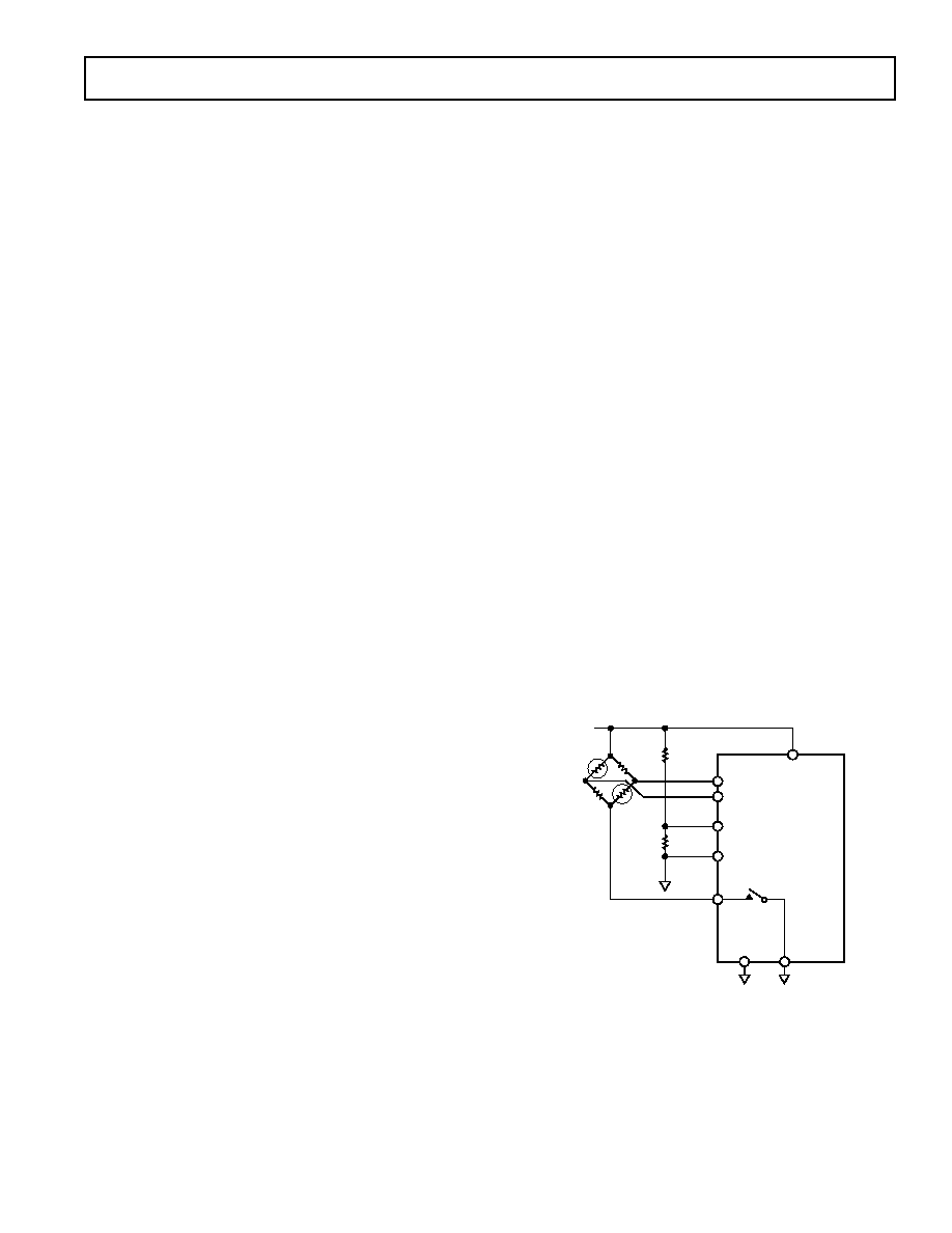
Pressure Measurement
One typical application of the AD7709 is pressure measurement.
Figure 18 shows the AD7709 used with a pressure transducer,
the BP01 from Sensym. The pressure transducer is arranged in
a bridge network and gives a differential output voltage between
its OUT(+) and OUT(–) terminals. With rated full-scale pres-
sure (in this case 300 mmHg) on the transducer, the differential
output voltage is 3 mV/V of the input voltage (i.e., the voltage
between its IN(+) and IN(–) terminals).
Assuming a 5 V excitation voltage, the full-scale output range
from the transducer is 15 mV. The excitation voltage for the
bridge can be used to directly provide the reference for the ADC
as the reference input range includes the supply. Alternatively, a
suitable resistor divider can be implemented that allows the full
dynamic range of the input to be utilized in this application.
This implementation is fully ratiometric, so variations in the
excitation voltage do not introduce errors in the system. Choosing
resistor values of 10 k
W and 6 kW as per Figure 18 gives a 1.875 V
reference voltage for the AD7709 when the excitation voltage is 5 V.
AD7709
IN+
OUT+
OUT–
IN–
10k
EXCITATION VOLTAGE = 5V
VDD
AIN1
AIN2
REFIN1(+)
P1
PWRGND
GND
REFIN2(–)
6k
Figure 18. Pressure Measurement Using the AD7709
Using the part with a programmed gain of 128 results in the
full-scale input span of the AD7709 being 15 mV, which corre-
sponds with the output span from the transducer.
相关PDF资料 |
PDF描述 |
|---|---|
| VE-230-MX-F1 | CONVERTER MOD DC/DC 5V 75W |
| LTC2250CUH#TRPBF | IC ADC 10BIT 105MSPS 3V 32-QFN |
| VE-22W-MX-F4 | CONVERTER MOD DC/DC 5.5V 75W |
| VE-22W-MX-F3 | CONVERTER MOD DC/DC 5.5V 75W |
| VE-22W-MX-F2 | CONVERTER MOD DC/DC 5.5V 75W |
相关代理商/技术参数 |
参数描述 |
|---|---|
| AD7709BRU-REEL | 功能描述:IC ADC 16BIT SIGMA-DELTA 24TSSOP RoHS:否 类别:集成电路 (IC) >> 数据采集 - 模数转换器 系列:- 标准包装:1,000 系列:- 位数:16 采样率(每秒):45k 数据接口:串行 转换器数目:2 功率耗散(最大):315mW 电压电源:模拟和数字 工作温度:0°C ~ 70°C 安装类型:表面贴装 封装/外壳:28-SOIC(0.295",7.50mm 宽) 供应商设备封装:28-SOIC W 包装:带卷 (TR) 输入数目和类型:2 个单端,单极 |
| AD7709BRU-REEL7 | 制造商:Analog Devices 功能描述:ADC Single Delta-Sigma 105sps 16-bit Serial 24-Pin TSSOP T/R 制造商:Analog Devices 功能描述:ADC SGL DELTA-SIGMA 0.105KSPS 16BIT SERL 24TSSOP - Tape and Reel |
| AD7709BRUZ | 功能描述:IC ADC 16BIT SIGMA-DELTA 24TSSOP RoHS:是 类别:集成电路 (IC) >> 数据采集 - 模数转换器 系列:- 标准包装:1 系列:microPOWER™ 位数:8 采样率(每秒):1M 数据接口:串行,SPI? 转换器数目:1 功率耗散(最大):- 电压电源:模拟和数字 工作温度:-40°C ~ 125°C 安装类型:表面贴装 封装/外壳:24-VFQFN 裸露焊盘 供应商设备封装:24-VQFN 裸露焊盘(4x4) 包装:Digi-Reel® 输入数目和类型:8 个单端,单极 产品目录页面:892 (CN2011-ZH PDF) 其它名称:296-25851-6 |
| AD7709BRUZ | 制造商:Analog Devices 功能描述:IC ADC 16-BIT SIGMA DELTA |
| AD7709BRUZ-REEL | 功能描述:IC ADC 16BIT SIGMA-DELTA 24TSSOP RoHS:是 类别:集成电路 (IC) >> 数据采集 - 模数转换器 系列:- 标准包装:1,000 系列:- 位数:16 采样率(每秒):45k 数据接口:串行 转换器数目:2 功率耗散(最大):315mW 电压电源:模拟和数字 工作温度:0°C ~ 70°C 安装类型:表面贴装 封装/外壳:28-SOIC(0.295",7.50mm 宽) 供应商设备封装:28-SOIC W 包装:带卷 (TR) 输入数目和类型:2 个单端,单极 |
发布紧急采购,3分钟左右您将得到回复。